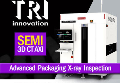
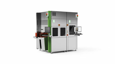
Automatic test and inspection solutions provider Test Research, Inc. (TRI) has launched the a 3D CT AXI solution for advanced packaging applications. The...

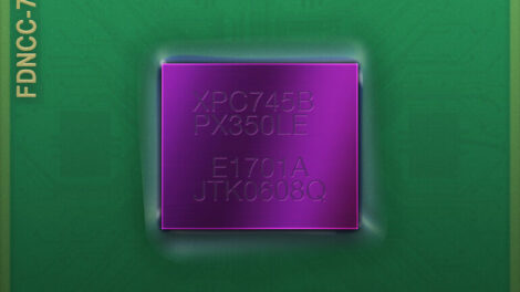
Semiconductor Packaging
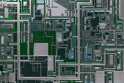
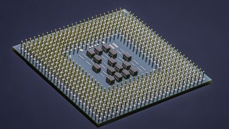
Semiconductors are a key strategic component in any industrial chain.
Source: Pixabay
The race for the most advanced semiconductors can only be won with technological and industrial leadership. Alongside the traditional mass business, the main drivers are high-tech applications such as Autonomous Driving, Edge Computing, IoT/IIoT, 5G/6G and Artificial Intelligence.
With increased demand, the need for innovative packaging solutions is rapidly growing. The EU has responded and is promoting the expansion of corresponding infrastructures in Europe with the European Chips Act. On this page you will find the latest news and information on all facets of semiconductor packaging.
News
TopLine Corporation, a developer of a wide range of advanced electronic packages for PCB assemblies, has filed for a patent for Indium-Niobium solder columns...

Find out more
Miniaturization continues. How does the border shift between SMT and Semiconductor Packaging proceed? What are the solutions for OSATs and SMT manufacturers...
Packaging holds the key for the further implementation of Moore’s Law. The chances are better than ever that Germany and Europe will play an even more...
News
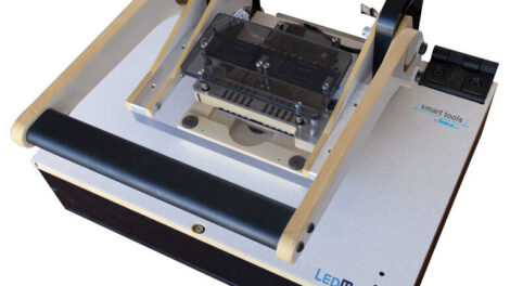
Canavisia, part of the Seica SpA group, exhibited its latest series of Smart Tools for electronics designers, test and production engineers at Embedded World 2024, which...
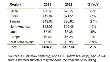
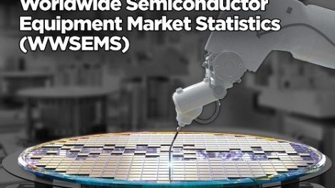
Worldwide sales of semiconductor manufacturing equipment edged down 1.3% to USD 106.3 billion (EUR 98.96 billion) in 2023 from an all-time record of USD 107.6 billion in...

Aiming to help the global semiconductor workforce expand its skills to address the talent gap, SEMI has announced the expansion of the SEMI University learning platform...
Henkel has commercialized a semiconductor capillary underfill encapsulant to address the requirements of the market’s most demanding advanced packages, like those used...
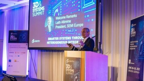
Leading experts in 3D integration and systems for semiconductor manufacturing applications will gather at the annual SEMI 3D & Systems Summit, 12–14 June, 2024, in...

Moov, the world’s largest marketplace for pre-owned semiconductor equipment, has announced plans to increase its headcount in Europe in 2024 to better serve...
Indium Corporation has designed materials solutions for semiconductor packaging and assembly to meet the evolving challenges of heterogeneous integration and assembly...
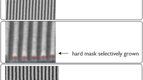
Imec, a research and innovation hub in nanoelectronics and digital technologies, has presented an overview of advanced node lithography and etch related processes that...
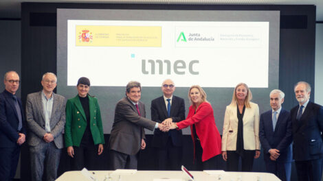
The Spanish government, together with the regional government of Andalusia and imec, an international research and innovation hub in nanoelectronics and digital...
SEMI, the industry association serving the global electronics manufacturing and design supply chain, has elected four new Semiconductor Climate Consortium (SCC)...

Siemens Digital Industries Software is adding accelerated pre-silicon development in the cloud to its hardware-assisted verification product offering with PAVE360...

The UK has joined the Chips Joint Undertaking, an EU semiconductor research initiative launched in late 2023 to address semiconductor shortages and strengthen Europe‘s...

The increasing complexity of electronics manufacturing requires embracing data analytics to manage electronics factories, according to a new white paper from IPC’s...

Nordson Electronics Solutions, a global leader in reliable electronics manufacturing technologies, has announced it offers plasma treatment and automated fluid...
Siemens Digital Industries Software has announced it has joined the Semiconductor Education Alliance to help build and nurture thriving communities of practice across...

Imec, a research and innovation centre for nanoelectronics and digital technologies, has launched its open process design kit (PDK) with a concomitant training program...

Semiconductor giant Intel is seeking to raise $2bn (€1.86bn) in equity to fund a new semiconductor fabrication facility in Ireland, according to a report by Bloomberg...
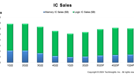
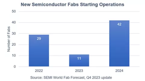
The global semiconductor manufacturing industry saw electronics and IC sales increase in the final quarter of 2023 with more growth projected for 2024, SEMI has reported...
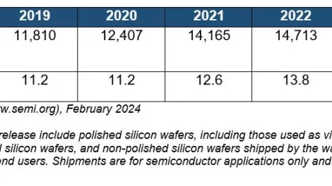
Worldwide silicon wafer shipments in 2023 decreased 14.3% to 12,602 million square inches while wafer revenue contracted 10.9% to USD 12.3 billion (EUR 11.4 billion)...

The EU‘s research partnership on semiconductors, the Chips Joint Undertaking (JU), is launching a joint call with South Korea as part of three new calls with a total...
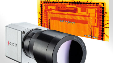
Electronic components consist of ever smaller structures and have a very compact design. Optris is now launching new microscope optics for the PI 640i infrared camera in...
The 10th IEEE Electronics System-Integration Technology Conference will be held in Berlin from 11–13 September 2024. IEEE ESTC is the premier international event in...
Infineon Technologies, a global semiconductor leader in power systems and IoT, and Wolfspeed, a global leader in silicon carbide technology, has announced the expansion...
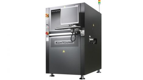
Koh Young Technology will present on its Multimodal Phase Shift Optics Approach to high-speed 3D reconstruction of semiconductor and advanced packages at the SMTA...
Global semiconductor capacity is expected to increase 6.4% in 2024 to top the 30 million *wafers per month (wpm) mark for the first time after rising 5.5% to 29.6 wpm in...

Provider of coating technologies Peters has announced it is contributing a 2-component primer FP 1321–1029 to the MID4automotive research project funded by by the...

US leaders in semiconductor design technology Synopsys and Ansys have announced that they have entered into a definitive agreement under which Synopsys will acquire...

Semiconductor giants Infineon, Intel and TSMC have all recently announce plans to build chipmaking facilities in eastern Germany with the support of government subsidies...
The SEMI Semiconductor Climate Consortium (SCC) has issued its first report of the semiconductor ecosystem’s greenhouse gas (GHG) emissions profile, an in-depth...
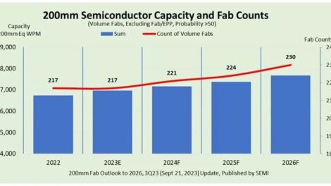
Semiconductor manufacturers worldwide are projected to increase 200mm fab capacity by 14% from 2023 through 2026, adding 12 new 200mm volume fabs (excluding EPI) as the...
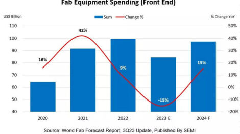
Global fab equipment spending for front-end facilities in 2023 is expected to decline 15% year-over-year (YoY) to USD 84 billion (EUR 79 billion) from a record high of...
Organisers of this year’s SEMICON Europa expo, co-located with productronica in Munich on 14–17 November, have announced that this year’s programme will include...

German engineering and technology giant Bosch has acquired U.S. chipmaker TSI Semiconductors, based in Roseville, California. The company originally announced its...

The world‘s largest manufacturer of semiconductors TSMC will invest USD 3.8 billion in a joint project with three other European industrial companies to build a...
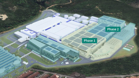
Infineon Technologies will invest EUR 5 billion over the next five years to expand its fab in Kulim, Malaysia into what it calls "the world’s largest 200-millimeter...

Infineon Technologies and German manufacturer of power semiconductor components Semikron Danfoss have signed a multi-year volume agreement for the supply of...
Worldwide silicon wafer shipments increased 2.0% quarter-over-quarter to 3,331 million square inches in the second quarter of 2023, the SEMI Silicon Manufacturers Group...
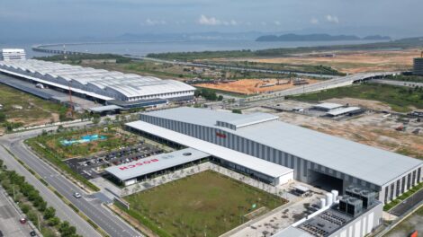
Global supplier of technology and services Bosch has opened an advanced semiconductor backend site in Penang, Malaysia for the testing of its automotive chips and...
Industry association SEMI has announced its intention to support the India Semiconductor Mission (ISM) in creating a vibrant semiconductor manufacturing and design...
Heraeus Electronics has announced its participation in the EU-funded research project ALL2GaN (Affordable smart GaN IC solutions for greener applications). This...

Supplier of mixed-signal automotive semiconductors Elmos Semiconductor SE has agreed to sell its wafer fab at the Dortmund site to US electronics manufacturing company...
Semiconductor supplier and provider of high-speed optical networking for harsh environments KDPOF has announced that the European Commission has granted it access to the...
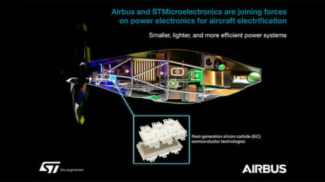
Airbus and STMicroelectronics have signed an agreement to cooperate on power electronics Research & Development to support more efficient and lighter power...

US manufacturer Intel has announced plans to construct a new semiconductor assembly and test facility near Wrocław in Poland. The company will invest up to USD 4.6...
Global industry association representing the electronics manufacturing and design supply chain SEMI has reported that the global semiconductor materials market revenue...
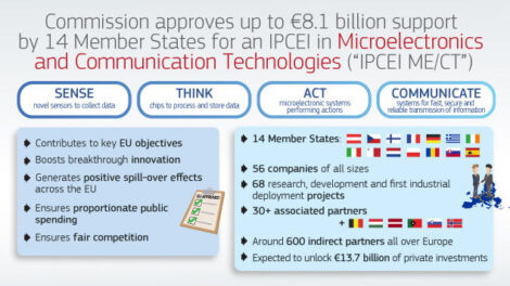
The European Commissioner Executive Vice-President Margrethe Vestager has approved an Important Project of Common European Interest (IPCEI) to support research...
Manufacturer of PCBs and IC substrates AT&S has taken a major step towards realizing a novel system integration approach, whereby D-Band chips and waveguides are...
The Electronic System Design (ESD) Alliance, a SEMI Technology Community representing members in the electronic system and semiconductor design ecosystem, has...
The European Commission has launched a pilot project known as the Semiconductor Alert System intended to monitor the semiconductor supply chain and warn of potential...

Infineon Technologies has signed an agreement with Chinese silicon carbide (SiC) supplier SICC to diversify its SiC material supplier base and to secure additional...

ZF and Wolfspeed have announced plans to jointly establish a European R&D centre for Silicon Carbide power electronics in the Nuremberg Metropolitan Region as part...
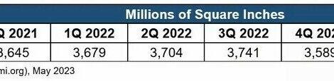
Worldwide silicon wafer shipments slipped 9.0% quarter-over-quarter to 3,265 million square inches in the first quarter of 2023 and 11.3% from the 3,679 million square...
Sony Semiconductor Solutions Corporation (SSS) has announced it has made a strategic investment in Raspberry Pi Ltd. (RPL), a UK-based maker of small single-board...
SEMI, the industry association serving the global electronics design and manufacturing supply chain, has announced that SEMI Europe, as the lead of a new 18-partner...
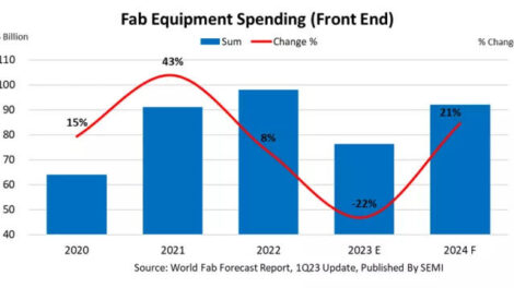
Global fab equipment spending for front-end facilities is expected to decrease 22% year-over-year (YoY) to USD 76 billion (EUR 70.4 billion) in 2023 from a record high...
The success of the CHIPS for America program depends on establishing a U.S. pilot facility for manufacturing integrated circuit (IC) substrates; and getting it done...

The government of the Netherlands has confirmed it plans to introduce restrictions on exports of microchip technology, following similar curbs introduced by the U.S in...
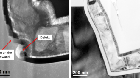
German research institute, Fraunhofer Institute for Microstructure of Materials and Systems (IMWS) says it has contributed to process and reliability optimisation of...

Industry intelligence provider Supplyframe Commodity IQ says supply-demand balance will normalize as the year advances, and that pricing and availability challenges will...
Industry association serving the global electronics manufacturing and design supply chain SEMI has announced that members of its Supply Chain Management (SCM) Initiative...
Advances driving the next generation of medical, environmental and mobility applications will take centre stage on 23–24 May at the SEMI MEMS and Sensors Technical...

The European Association of Automotive Suppliers (CLEPA), which represents over 3,000 companies supplying components and technologies for mobility, has released a...
Research and innovation hub in nanoelectronics and digital technologies Imec has it has demonstrated co-integration of its high-quality silicon nitride waveguide...
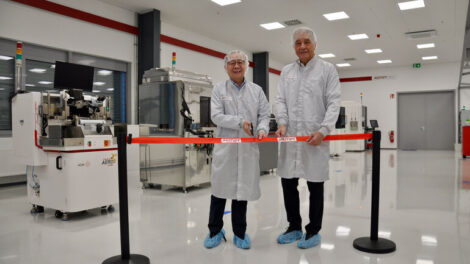
ASMPT, a leading provider of hardware and software solutions for semiconductor and electronics manufacturing, has opened its first European semiconductor Center of...

US maker of power chips Wolfspeed Inc. will invest over EUR 2 billion to build the world‘s largest factory for silicon carbide (SiC) semiconductors in Saarland...

The UK government will provide taxpayer funding to support British semiconductor companies as part of a strategy to promote domestic chip manufacturing, and diversify...
Industry association SEMI has announced that its Semicon West microelectronics exhibition and conference, which has been held in San Francisco Bay for more than 50...

Semiconductor test equipment supplier Advantest Corporation has announced it will feature its latest test solutions for advanced ICs at the Semicon Korea event on...
Electronic System Design (ESD) industry revenue increased 8.9% from USD 3,458.2 million in Q3 2021 to USD 3,767.4 million (EUR 3,459 million) in Q3 2022, the ESD...
Industry association SEMI has announced that the European Chips Act and Europe’s leading-edge R&D capabilities – both key drivers of Europe’s microelectronics...
New Axion T2000 Extends Advanced Metrology Portfolio That Addresses Vertical Scaling Challenges in Memory Chip Manufacturing.
KLA Corporation announced the launch of...
Infineon Technologies AG is increasing its target operating model and reporting its results for the fourth quarter and for the full fiscal year, both of which ended on...
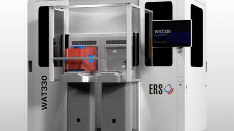
ERS electronic, a leading supplier in thermal management solutions for semiconductor manufacturing, upgrades its Warpage Adjustment Tool (WAT330), to include...

Company broadens portfolio to include next-generation substrates and panel-level processes for heterogeneous semiconductor solutions
Lam Research Corp. announced that...
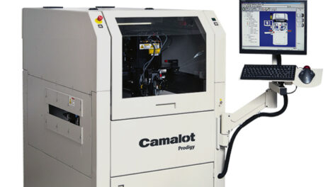
ITW EAE is releasing a proprietary syringe cooling option that increases the “pot-life” of underfill materials by maintaining the syringe at controlled temperature...
KLA Corporation introduced the new Orbotech Corus 8M direct imaging (DI) solution, the first system built on the all-in-one revolutionary Orbotech Corus platform...

The Taiwanese semiconductor company TSMC is pushing ahead with plans for its own production in Germany. According to information from the business magazine CAPITAL, a...

STMicroelectronics will build an integrated Silicon Carbide (SiC) substrate manufacturing facility in Italy to support the increasing demand from ST’s customers for...
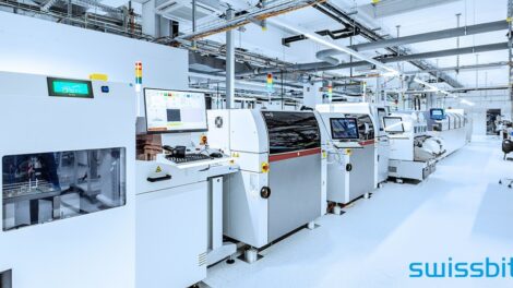
Swissbit is continuing with its strategic expansion plans at its established production facility in Berlin, Germany by adding a new semiconductor packaging line to its...

A consortium of Fraunhofer institutes and well-known German industrial companies is developing a split-manufacturing approach for semiconductor production in the project...
KLA Corporation has announced plans to build a new research-and-development (R&D) and manufacturing center for the SPTS division, in Newport, Wales, UK. The new...

Two years ago, our Institute’s site in Moritzburg – the »All Silicon System Integration Dresden – ASSID« - was able to celebrate a decade of successful work...
Siemens Digital Industries Software today announced it has collaborated with leading semiconductor foundry United Microelectronics (UMC) to develop and implement a new...

The 9th Conference on Technology for the Integration of Electronic Systems (ESTC 2022) was held in Sibiu from 13-16th September 2022.
ESTC is one of three premium...

Split manufacturing for trustworthy electronics "Made in Germany"
A consortium of Fraunhofer institutes and well-known German industrial companies is developing a...
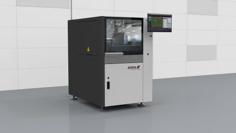
EV Group (EVG), a leading provider of wafer bonding and lithography equipment for the MEMS, nanotechnology and semiconductor markets, introduced NanoCleave, a...
Henkel announced the commercialization of its latest semiconductor-grade capillary underfill (CUF) formulation for advanced packaging applications. The material, Loctite...
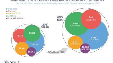
The top 8 advanced packaging players dominate the market and continue with heavy investment.
• The advanced packaging industry is expected to have a 9.6% CAGR...
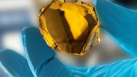
At German based Fraunhofer Institute for Integrated Systems and Device Technology (Fraunhofer IISB) an aluminum nitride (AlN) crystal with a diameter of 43 mm in...
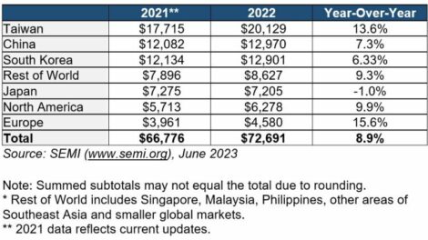
Global semiconductor equipment billings rose 7% from the first to the second quarter of 2022 and 6% year-over-year to US$26.43 billion, SEMI announced today in its...
It is well known that modern paste printing systems are characterised by their high flexibility: The printing systems adapt dynamically to changing requirement profiles...

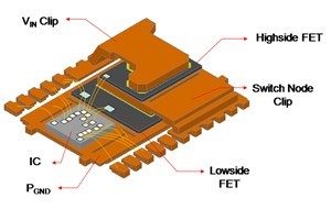
MacDermid Alpha Electronics Solutions, a global supplier of advanced solutions for power electronics and semiconductor applications, introduces a new packaging option...
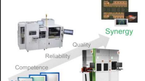
To be able to migrate from precision placement of SMD to Semiconductor packaging a knowledge transfer in several areas of the supply chain is going to take place. We...

Palomar Technologies, a global supplier of total process solutions for advanced photonics and microelectronic device packaging, has appointed Mr. Thorsten Scheidler as...
ASYS, Christian Koenen and Koh Young Europe, supported by EPP Europe part of Konradin publishing group, will present innovative solutions for semiconductor packaging at...
The 9th ELECTRONICS SYSTEM-INTEGRATION TECHNOLOGY CONFERENCE (ESTC 2022) will take place in-person in Sibiu (Hermannstadt), Romania, in less than a month. ESTC is the...
Due to the shortage of components in the electronics industry and the dependence on Asian suppliers, the European Community has decided to double Europe's global market...
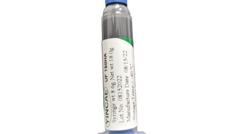
YINCAE is announcing UF 158HA that is fully compatible with flux residue and high performance underfill. Using UF 158HA can eliminate cleaning process and pollution from...
To be able to migrate from precision placement of SMD to Semiconductor packaging a knowledge transfer in several areas of the supply chain is going to take place. We...

Intel Corporation announced that Lip Bu Tan, executive chairman of Cadence Design Systems Inc., chairman of Walden International, and founding managing partner of...