To be able to migrate from precision placement of SMD to Semiconductor packaging a knowledge transfer in several areas of the supply chain is going to take place. We believe that soon many SMD manufacturer will also produce components and supposed to be able to manufacture mid-size or even high quantity batches.
With this newsletter we like to support SMD and Semiconductor manufacturing with information about very efficient, high performance print processes for Semiconductor Packaging. In the coming months we will share experience specifically about the following topics:
Semiconductor Backend Processes
- Bumping
- Balling
- Flux printing
- Chip assembly
- Chip stack assembly
- Pre-bowed Chip assembly
- Copper Pillar chip assembly
- Chip moulding and filling
- Conventional LED assembly
- Min-LED assembly
Chip assembly Process
The difference between wafers and chips lies in the relationship between both components. While the wafer serves as a base for the chip, the chip is implanted in the wafer. Together, they make up the integral part of Semiconductor components that’s commonly used in the field of electronics.
Microchips are made by building up layers of interconnected patterns on a silicon wafer. The microchip manufacturing process involves hundreds of steps and can take up to four months from design to mass production. The process of putting a semiconductor device or integrated circuit in a package of one form or another usually consists of a series of packaging steps that include: die preparation, die attach, wirebonding, encapsulation or sealing, deflash, lead trimming/forming, and lead finish.
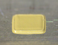
Microchips are often flat bonded onto a Leadframe or substrate. This flat bonding process is done by adhesive or sinter materials. High speed dispensing processes are often used to place the right amount of bonding deposit accurately onto substrates. This is a sequential process and requires several seconds per Microchip. Because the amount of chips / Wafer is continuously increasing, Semicon manufacturer have moved to the more economical and fully automatic high speed precision stencil printing process. Print processes will be exponential faster, because the number of deposits is not influencing the process time and the required level of printing process quality can be achieved by customized “Semicon Stencil” designs. Beside the speed and cost improvements there will be also a benefit in print process repeatability.
By using a dispenser, usually a shamrock shape deposit will be placed. This shamrock shape will have as well a tail in the middle which makes is much higher as the dispens needle usually is. The chip then get pressed down into the deposit to the required wet BLT (Bond Line Thickness) and the excessive paste or glue gets pushed out sidewards. This is hardly controlable and the risk of conections to other comonents , or even to move on top of the dice is there. Volume tolerances of dispenser deposits are sometime up to 40% of the nominal placed volume.
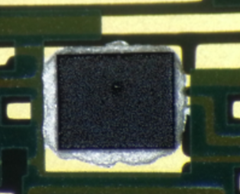
By using a High precision stencil print process, the shape of the deposits will be flat and perfectly shaped for the contour of the Semiconductor Chip. By printing the deposit just higher as the wet BLT should be and the right contour, there will be almost no excessive paste pushed out to the side. Also, the tilt of the dice is limited due to the flat deposit. Boosting the productivity and increasing the quality yield by using a high precision print process is possible due to the parallel processing of all required deposits and higly repeatable. Usually print process defined volumes are in a tolerance of about +/-5% of the nominal volume.
Our Semicon teams at Christian Koenen GmbH have extensive process knowledge to design and manufacture customized Semicon stencils. We are offering service support to perform and test printing processes in our Application Lab. Together with our customers we often perform extensive analysis and checks to prove and prepare printing processes for mass production.
State of the art process equipment and measurement methodology is available to establish and optimize all kind of Wafer printing processes. Please contact our team as soon as you like to learn more about stencil printing for Semicon manufacturing processes.
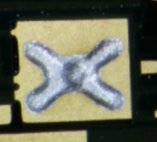
(excessive paste overflow at the outside)