German research institute, Fraunhofer Institute for Microstructure of Materials and Systems (IMWS) says it has contributed to process and reliability optimisation of gallium nitride (GaN) devices by discovering a new defect signature in GaN components, as part of its work in the EU-funded project known as Ultimate GaN.
In the recently completed research project, which ran for 3.5 years from 2019 to 2022, a consortium of 26 European partners from science and industry, under the leadership of Infineon Austria, set themselves the task of harnessing the advantages of GaN technology along the entire value chain, from process development, design, assembly and interconnection technologies to integrated system solutions.
While GaN-based power semiconductors offer higher performance in a smaller space, and thus save energy and resources, the special chemical-physical material properties and the structure of high-electron mobility transistors raises questions. “The high electric field strengths and enormous current and power densities with correspondingly high material stress in these very compact components pose particular challenges.“, explained Frank Altmann, Head of the Business Unit ‚Materials and Components for Electronics‘ at the Fraunhofer IMWS.
With high-resolution analysis procedures and innovative fault diagnosis methods the Fraunhofer Institute for Microstructure of Materials and Systems IMWS contributed to process optimisation and increasing the reliability of the GaN devices.
“We are researching specific critical defects or GaN-specific degradation processes in order to be able to detect, understand and thus avoid new failure modes as early as possible,“ said Altmann.
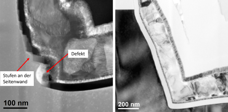
Leakage current paths, for example, were localised after reliability testing and investigated microstructurally to determine their cause. As such, a new defect signature was identified that led to the premature electrical breakdown of special semi-vertical GaN transistors. On the basis of these findings, the manufacturing process could be systematically optimised.
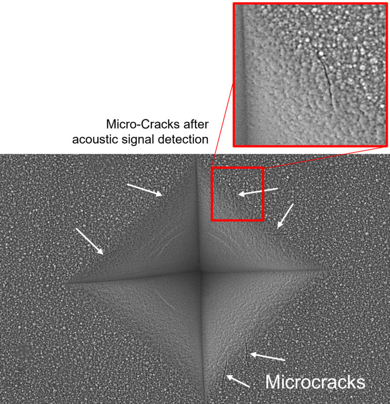
With nanoindentation testing in combination with acoustic emission, IMWS scientists were able to detect hidden microcracks under the metallisation layers of bond pads. The above mentioned methodology was applied and evaluated on different processed samples of the project partners and the related defect structures were investigated by electron microscopy analyses.


