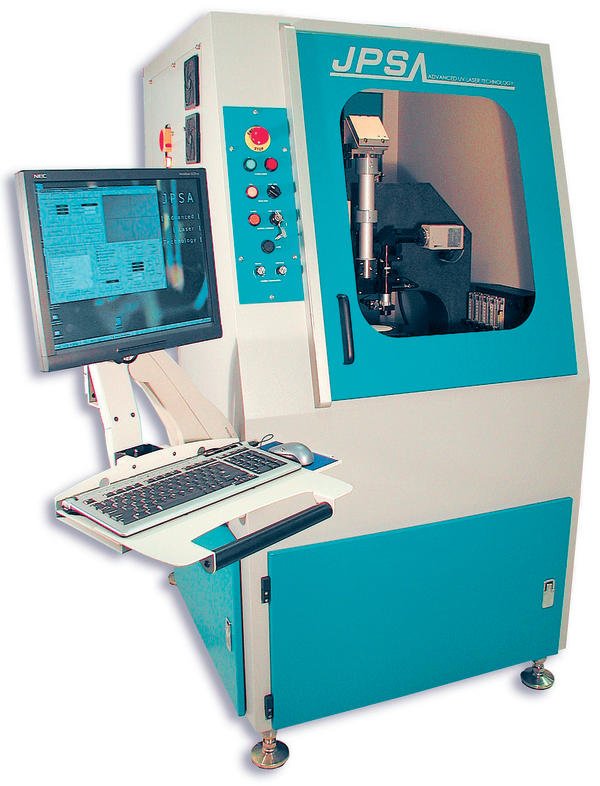
The IX-4000 series laser workstations from J. P. Sercel Associates (JPSA) are available in both DPSS (solid state) and excimer laser configurations. The IX-4500 ChromaDice solid state laser machining system delivers high speed wafer singulation integrated with a wafer loading system. Featuring dual SMIF or FOUP load ports, the system is ready for the most demanding wafer die singulation production task. It features low operation costs per wafer, > 99 % process yields combined with narrow kerf widths. Available with wavelengths from 1064 nm to 266 nm, the system is ready for processing a variety of materials, from Si to Sapphire and, when equipped with the Company’s patent pending Toxic Wafer Debris nozzle, materials such as GaAs and InP are handled with ease.
The IX-4000 ChromAblate is an excimer laser version for LED liftoff, via drilling, micro-machining, thin film patterning and other semiconductor packaging applications. Whether micro-machining features to 2 µm or configured for large area exposure of up to 5 mm x 5 mm, the excimer laser version is engineered for 24/7 industrial production with a high degree of flexibility and configurability. The system features dual cassette loading ports, production-grade robotics, wafer pre-aligners and vision, all combined in a user-friendly class I laser system. Applications include laser lift-off, selective wafer annealing, micro-drilling, dicing and scribing, ink jets, via drilling, blind holes, micro-fluidics, thin film patterning, selective material ablation, MEMS, 3-D micro-machining, fire-on-the-fly operation and more.
Features include full automation, including part load/unload robotics, pre-aligners and vision system for unattended production. A variety of standard and custom end effectors are available for any part-handling requirement; compact design; modular configuration; plus high accuracy, with linear motor air bearing stages providing accuracies to less than 2 μm. The excimer laser version also offers a large workspace, as it can be configured with stages able to handle wafers up to 300 mm. Additionally, it provides a uniform beam profile, with a variety of imaging and non-imaging homogenizers available for large-area applications.
EPP Europe 438
Share:
