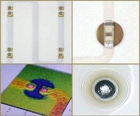
By utilizing stencil-printing and enclosed print-head material deposition, DEK has implemented cost-effective and yield-enhancing bumping and ball-placement process alternatives to traditional methods. For bumping at wafer and substrate levels, a print and reflow method is employed that allows for single stroke, virtually unlimited bump quantity with height targets of 80 to 150 microns on pitches of 150 up to 500 microns. This technique requires strict application of design rules when creating the stencil, which is generally electroformed. Also imperative to the success of this method is the design of the bond pads to allow sufficient contact area to achieve good solder-joint strength for a given standoff. The enabling technologies that allow printing platforms to be configured to meet these semiconductor packaging requirements include automated wafer-handing, cleanroom-compatible paperless cleaning and an enclosed print head (ProFlow), delivering accurate paste volumes. When pitch and bump size is appropriate, placing instead of forming solder bumps at wafer and substrate levels is an alternative. The DirEKt Ball Placement solution can place solder balls of 0.3mm in diameter, with fine-pitch accuracy and first-pass yields consistently better than 99%. Using a sophisticated flux-imaging technology, the wetting agent is deposited at each interconnect site. Then, the ProFlow transfer-head guides each solder ball directly to the surface of the stencil, and a controlled placement force seats each sphere into the flux. Cycle time is claimed to be incredibly fast and completely independent of I/O count. Reportedly, these mass-imaging methods are effectively delivering the increased performance and lower investment costs that packaging specialists are demanding.
EPP EUROPE 440
Share: