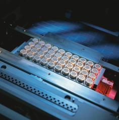
Recognizing that individual processing of chip packages is inefficient and traditional, and that multiple package processing using dispensing can be slow and defect-ridden, DEK has developed an innovative, robust multiple package solution that is claimed to dramatically decrease cycle time while delivering unmatched accuracy and repeatability. This singulated substrate system can be used to process multiple packages in the same cycle. Enabled by Virtual Panel Tooling (VPT) technology, parts can be fed into the printing system in JEDEC-format carriers, and simultaneous processing of individual substrates of varying sizes can occur. Because the advantages of high-accuracy mass imaging and full capabilities of the stencil printer can be utilized, VPT enables a more seamless crossover between the two arenas of assembly and expands packaging capabilities through increased throughput and yield. This process is ideally suited to high-accuracy or ultra-fine pitch applications such as substrate solder bumping, epoxy printing for die-attach, thickfilm-substrate manufacture, fluid dispense and other relevant applications. This process reportedly results in record-breaking throughput levels while maintaining precision, repeatability and accuracy in alignment and print deposition. VPT aids in cost-effective package manufacturing, significantly reducing costs, and has been qualified for printing 220µm-pitch devices, conductive epoxy for slug attach, ball attach and full pin-grid array for passive component assembly. Throughput can be multiplied by increasing the number of substrates in each carrier, which delivers an even greater return on machine investment and reduces the number of systems required to achieve the desired production volume.
EPP EUROPE 452
Share:
