The coatings and varnishes on electronic assemblies must adhere perfectly to ensure optimal functionality even under extreme adverse conditions. Therefore, highest requirements are placed on the surface cleanliness of assemblies. To meet these requirements, EADS Deutschland GmbH introduced a new cleaning process for assemblies. This article describes the requirements, which EADS addressed to the process, and how the evaluation of the new cleaning process was conducted. In addition, this case study illustrates how the company was able to meet the requirements for surface cleanliness prior to coating due to this cleaning approach.
EADS (European Aeronautic Defense and Space Company) Deutschland GmbH can look back on many years of corporate history. Since its foundation in 1903 under the name of Telefunken, the company has undergone several name changes and carries the name EADS since July 2000. EADS is the world’s second largest company in the aeronautics, aerospace and defense industry with approximately 90 locations and around 110,000 employees worldwide. Defense Electronics (DE), the sensor and avionics division of EADS (with approximately 2500 employees) offers its customers components, equipment and subsystems based on cutting-edge radar and electronic warfare technologies. Innovative Defense Electronics products are not only used in EADS own platforms, but also compatible with fighter, mission and transport planes, helicopters, tanks and ships by other manufacturers.
The necessity of assembly cleaning at EADS
Whereas cleaning after soldering rarely occurs in the high-throughput production of SMT assemblies with minimum requirements on reliability, sensitive applications frequently require cleaning due to high standards of product reliability. Conformal coatings in particular require a residue-free surface, which can only be achieved with appropriate cleaning processes. Since the coating of the assembly is generally the last step in the chain of added value, errors in this production step can have a drastic effect on production costs and lead to disastrous field failures. For example resin residues, which are not cleaned off prior to coating, can cause delamination or cracks in the protective coating. In addition, activator residues can form electrolytes, which trigger electrochemical migration under the coating. Given the dominance of Defense Electronics in the area of high-reliability electronics, most of the manufactured assemblies belong to the conformal coating class. By introducing an optimal cleaning process at the Ulm manufacturing plant, several advantages were achieved over the previous cleaning process.
Requirements for the new cleaning process
The basic requirements for choosing a system were logistically optimized machine positioning and an acceptable cleaning medium in terms of working safety. By using water-based media, a critical flashpoint is no longer an issue as it is in the case of solvent-based systems, and protective measures are not required. Such a cleaning process is also much more acceptable and progressive from an environmental point of view. The new cleaning process must ensure that geometrically critical assemblies with fine pitch SMD and components with small standoffs are reliably cleaned.
Evaluating the new process
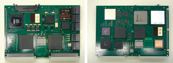
A large evaluation for an ideal cleaning process was carried out at Defense Electronics with the goal of determining a suitable cleaning method. Since the investigated test specimens had to mostly conform to representative assembly series, appropriate test boards were designed (figure 1). Various aspects were taken into consideration to justify the potentially critical points of assemblies, which can be very complex: The test substrates had a high integration density to gain information on thorough medium rinsing of complex contours, and cleaning performance in relationship to the soldering site density. In addition, flow-promoting “package monocultures” were avoided to duplicate real printed circuit board characteristics and avoid random preferences, which would only be representative of special structures. Innovative packages were used to give consideration to current developmental trends. THD (various plug-in connectors, switches) and SMD (plug-in connectors, QFP, tantalum capacitors, chips 0201, 0402, 0603, 0805, 1206) were used to duplicate typical printed circuit board structures from the product portfolio of Defense Electronics. Furthermore, ball grid arrays with different housing and ball sizes were used to compare the ability of cleaning in small standoffs.
The test substrates were populated with comb structures (in accordance with IPC-B-25 with 317/317 µm & HDI-SIR comb with 125/125 µm) for the optional, non-visual monitoring of the cleaning results using surface isolation resistance measurement. In addition, high-surface component geometries were simulated focusing on coating compatibility and flux residue characteristics. In addition to the comb structures, specific test areas were provided for cross-hatch testing to check the adhesion of different coatings according to DIN EN ISO 2409:
- Conformal coating with polyurethane varnish Conthane CE-1155 (2K) or Hysol PC18M (1K)
- Conformal coating with acrylic Humiseal 1B31
- Conformal coating with parylenes
During the test series, various combinations of equipment and cleaning agents were investigated for the best possible compatibility. The cleaning results were investigated both visually and through a light microscope with 25x enlargement, and contamination was measured to detect ionic impurities on the board level. Various evaluation criteria for the test results were selected:
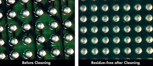
- Visual inspection according to IPC-A-610D / class 3:
- => No visible residues at the selected enlargement
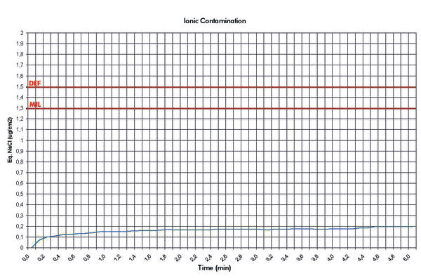
- Ionic contamination in accordance with DN EN 61191–1, section 9.5.6
- => Maintenance of maximum permitted concentration £1.56 µg/cm²
New cleaning approach
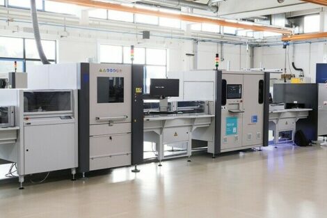
By combining a 71 W cleaning system (Dürr) with the cleaning agent Vigon A 200 (Zestron), an appropriate process was found for the investigated spectrum of products. The cleaning equipment is based on a single-chamber system, which is flooded with the cleaner from a media tank. The aqueous cleaner Vigon A 200 is used, which is based on the patented MPC or Microphase Cleaning Technology. While surfactant cleaners bond to contaminants, MPC cleaning agents precipitate the residues. The micro phases remove the contaminants from the substrate surfaces and transfer them to the surrounding aqueous phase. This technology presents the following advantages:
- The contaminants can be easily removed from the cleaning process using simple bath processing measures such as filtration.
- No selective depletion of active ingredients.
- Significantly longer bath life as well as lower process costs are achieved in comparison to solvent or surfactant cleaners.
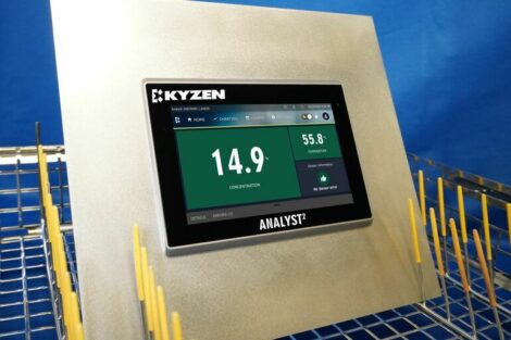
Cleaning can be supported by the addition of individual, freely selectable mechanical procedures (such as spray-in-air, spray-under-immersion, vacuum, ultrasonic, etc.). The cleaning step is followed by two rinsing steps with demineralized water to completely rinse off the cleaner. Finally, the assemblies are dried with hot air and/or vacuum assistance. This process fulfilled the two required acceptance criteria with sufficient reliability. The specification limits were met, and the cleaning results revealed typical values of ionic contamination far below the threshold of 1.56 µg/cm², even with critical boards (figure 2). The new cleaning process also met the cleanliness requirements for components with small standoffs and critical component geometries (such as BGAs) (figure 3). In the test series, which led to the selection of this combined process, Defense Electronics was able to access a wide variety of different cleaning systems and professional expertise at Zestron Europe. A majority of the evaluation trials were performed at Zestron’s Technical Center and the results were analyzed with corresponding analytical methods.
Conclusion
Excellent results have been achieved since the installation of the cleaning process. Not only did the cleaning process meet the process qualification requirements, it also provides consistent cleaning results and operates stable. The implementation of an aqueous cleaning process also increased the acceptance among the process operators as well as the persons responsible for the hazardous material and safety department. The provided support from the cleaning experts turned out to be of most benefit to Defense Electronics of EADS.
SMT, booth 7-225, 7-639/NEW UK, B 48
EPP Europe 433
zusammenfassung
Die Beschichtung/Lackierung elektronischer Baugruppen muss einwandfrei haften, um optimale Funktionssicherheit bei extremen Bedingungen zu gewährleisten. Daher bestehen höchste Anforderungen an die Oberflächenreinheit vor der Beschichtung. Um diese erfüllen zu können, hat die EADS Deutschland GmbH in ihrer Fertigung einen neuen Reinigungsprozess für Baugruppen eingeführt. Der Artikel beschreibt, welche Bedingungen an den Reinigungsprozess gestellt und wie die Evaluierung durchgeführt wurde.
Un revêtement/une peinture appliqué sur des blocs de composants électroniques doit adhérer parfaitement pour pouvoir assurer une sécurité de fonctionnement optimale à des conditions extrêmes. Par conséquent, la propreté superficielle doit être parfaite avant l’application. Pour satisfaire à cette exigence, la société EADS Deutschland GmbH a introduit un nouveau processus de nettoyage des blocs de composants sur ses chaînes de production. L’article décrit quelles sont les conditions devant être remplies par le processus de nettoyage et comment est effectuée l’évaluation.
Il rivestimento/la verniciatura dei componenti elettronici deve aderire perfettamente, per garantire un funzionamento corretto ottimale in condizioni estreme. Per questo i requisiti di pulizia della superficie prima del rivestimento sono molto elevati. Per ottenerli, EADS Deutschland GmbH ha introdotto nella propria produzione un nuovo processo di pulitura dei componenti elettronici. L’articolo descrive le condizioni richieste per la pulitura e come è stata effettuata la valutazione.
Share:


