The increased functionality of personal electronic devices has driven the need for miniaturization of components. This is happening simultaneously as the conversion to RoHS-compliant lead-free assembly, providing considerable challenges to the industry. The higher reflow process temperatures required for Pb-free assembly can thermally damage the PCB and components, and negatively affect solder joint quality. Low-temperature is solder advantageous in this process.
Brook Sandy-Smith, Edward Briggs and Ronald C. Lasky, Ph.D., Indium Corporation, Clinton, NY, USA
The base metal for most solders is tin, which melts at 232 °C. Bismuth is a low-cost alloying option that can be used to reduce tin‘s melting temperature. This paper considers 57Bi/42Sn/1Ag, and reviews studies conducted by Hewlett-Packard (HP), alongside new work. Studies performed by HP show that low-temperature BiSnAg has properties approaching or surpassing Sn63 (tin-lead solder) under most conditions1).
Wetting
Many factors affect wetting behavior, such as surface tension of solder, PCB pad metallization, and flux activity. Early work by HP 1) showed flux activity was vital and once the proper flux chemistry was achieved, the results of the spread test and wetting angle were near those of Sn63. Most tin-lead fluxes activate at 160 °C – 170 °C, which is too high for the BiSnAg process.
Shear
Solder joints experience shear stress caused by CTE (coefficient thermal expansion) mismatch in temperature cycling. The HP study found BiSnAg had a higher shear strength than Sn63 at 20 °C, comparable at 65 °C, and lower (but comparable) at 110 °C2).
Creep
Creep is defined as a constant load, causing deformation or flow over time. The steady state creep strain rates, as a function of shear stress, were evaluated at 25 °C, 65 °C, and 90 °C for BiSn and Sn63. These tests showed that the creep resistance of BiSn exceeds Sn63 at 25 °C – 65 °C1).
Thermal fatigue
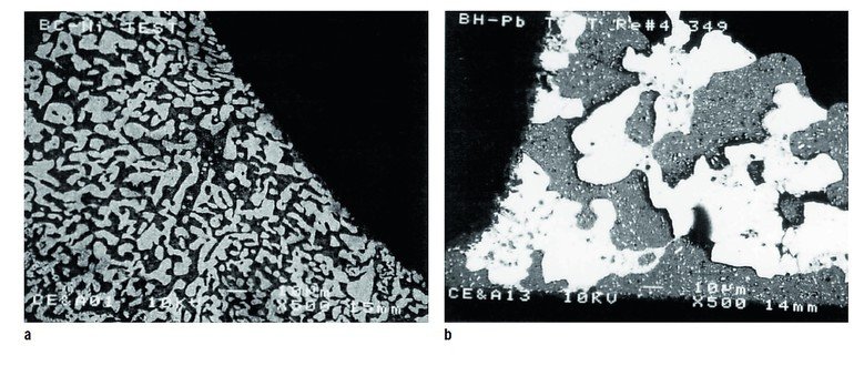
During HP’s thermal-fatigue testing all passed visual and functional testing, but during thermal cycling (-20 °C– 110 °C) thermal failure was observed with BiSn solder on the SnPb HASL-finished PCB pads. Before testing, all solder joint surfaces were smooth. Afterward, the SnBi on SnPb HASL was grainy, while the BiSn on CuOSP was still smooth. This roughness was due to large-grain growth, which HP concluded was due to Pb from the surface finish dissolving into the BiSn solder, forming a low-melting eutectic at 96 °C1). In later work, HP observed small additions of Ag/Au increased the thermal fatigue life of the BiSn alloy and suggested Ag may decrease the grain size and stabilize the microstructure4).
Bend test BGAs
In this test, plastic ball grid arrays (PBGAs) assembled with high tin-containing solder spheres (with liquidus ≥ 217 °C) did not melt/collapse using the low-temperature profile required for SnBi solder paste. Also, when the SnBi solder paste volume was insufficient, all solder joints failed between the PCB and the BGA ball. With adequate paste volume, the SnBi solder joint strength improved enough to force failure by pullout of tthe Cu pad, about ~65 % of Sn63 stress.4)
Summary of HP testing
BGAs: It was recommended to use SnBi/SnBiAg solder spheres so solder joints would collapse and improve joint microstructure, thus improving mechanical properties. Current Sn63 or SAC stencil aperture designs can be used. SAC alloy balls will not collapse due to the lower temperature reflow process associated with SnBi/SnBiAg alloys. Therefore, when using SAC solder spheres more paste is required than currrent stencil designs for Sn63 or lead-free processes deliver.
Backside components: SnBi/SnBiAg alloys have llower surface tension than Sn63 or lead-free alloys. TThis may be problematic in double-sided reflow for heavier components on the underside, as components may not be held in place during the second re-fflow.
Surface finishes: HP concluded that CuOSP PCB pad surface finishes consistently showed the best mechanical and process results. However ImAg, ENIG, and ImSn all produce acceptable wetting and subsequent performance.
Bake out: Post-baking procedures may need altering –90 °C for 12 – 15 hours should be sufficient.
Component placement: Lower surface tension of SnBi/SnBiAg alloys means component placement may be more critical, as less self-alignment may occur.
Depanelization: Use adequate fixturing and board support, as
BiSnAg has a more sensitive strain rate.2)
New study results
Printing
This experiment observed transfer efficiency of SnBiAg solder paste and noted any difference in process parameters from the typical Sn63 or lead-free solder pastes. To minimize variables, the same stencil, squeegee blades, and printer parameters were utilized as in previous experiments with Sn63 and Pb-free solder pastes.
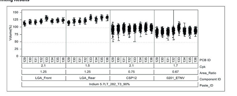
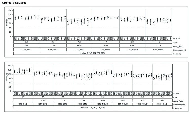
A 4 mil stencil, 250 mm wide squeegee, foil-less clamps, and landscape vacuum support blocks were used. Solder paste was printed at 50 mm/second squeegee speed with blade pressure of 4 kg. Test boards with 16, 14, 12 mil circular and square, (and 11 mil squares) were evaluated, as were 0201, land grid array (LGA), and various rectangles in both solder mask defined (SMD) and non-solder mask defined (NSMD) pads. A no-clean solder paste with type 3 particle size of 57Bi/42Sn/1Ag was chosen. Eight PCBs were printed with no stencil wipe, and the volume of the stencil-printed deposits was collected via a laser-scanning system.
Area ratio
The stencil aperture area ratio (AR) is a critical metric in stencil printing. It is the area of the stencil aperture opening divided by the area of the aperture side walls. A simple derivation shows AR = D/4t, where D is diameter and t is thickness. For a rectangular aperture, the formula is ab/2 (a+b) t, where a and b are the sides of the rectangle. For good stencil printing, the AR must be greater than 0.66. Transfer efficiency is defined as the volume of the solder paste deposit divided by the volume of the aperture.5)
SMD vs NSMD
For larger apertures ( 14 mil), the non-solder mask-defined (or pad-defined) PCB pads provided better transfer efficiency than the solder-mask defined. For the larger pads, the non-solder mask-defined pads provided a better stencil to PCB gasket. However, as the PCB pads became smaller ( 14 mil), the mask-defined pads provided better transfer efficiency. Paste release from the stencil aperture partially relies on adhesion of solder paste to the PCB pad. As the PCB is lowered from the stencil aperture, adhesion of solder paste to the PCB helps the paste “pull” out of the stencil aperture. With the smaller pad, there is little surface area for adhesion; the wall of the solder mask (mask-defined pad) may increase the surface area for adhesion, improving paste release.
In summary, the printing process for SnBiAg solder paste was very similar, if not identical, to the Sn63 or lead-free process.
Reflow profile results
Our reflow experiments used a ramp-to-peak profile with a peak temperature of 170 °C – 180 °C and time above liquidus (TAL) of 70 – 80 seconds. Lower processing temperatures often require a longer TAL to allow intermetallic formation.
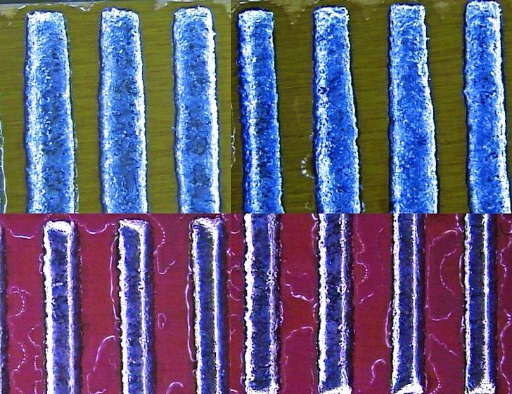
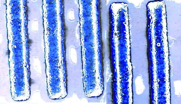
A common test vehicle was used with apertures of 38.5 mil x 390 mil and 90 mil pitch size. The paste was printed and reflowed on CuOSP-finished PCB pads immediately after printing, and then solder joints were evaluated. Additional samples were printed on ENIG, CuOSP, and ImAg PCB pads and placed in humidity chambers – the first sample for 3 hours at 76 % RH and the second for 3 hours at 90 % RH. Samples were then reflowed to observe humidity resistance in solder joint formation.
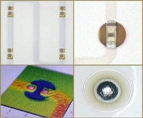
Solder ball
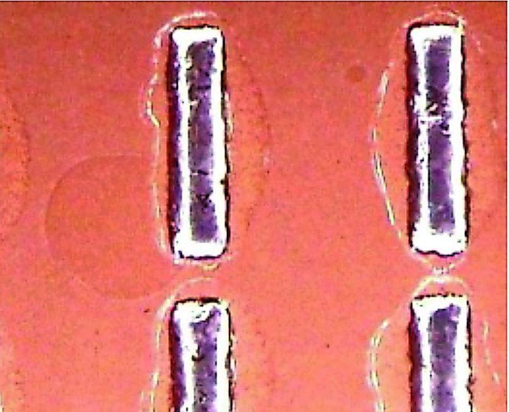
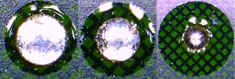
A test vehicle with 100 mikron CuOSP pads was selected. Solder balls typically increase if the printed solder paste deposit infringes onto the solder mask. To challenge the solder paste, stencil apertures were incorporated to purposely overprint onto the solder mask. Stencil apertures for the 100 microns pads were 75, 100, 125, 175, 225, and 275 microns.
The results were very favorable, with 1 solder ball at 225 microns stencil aperture (ratio 1.0/2.25) and 2 solder balls on the 275 microns stencil aperture (ratio 1.0/2.75).
Voiding
The test vehicle utilized 6 microns x 6 microns QFNs, ImAg finish, with via-on-pad. The solder paste was printed 1:1, reflowed and X-rayed to observe the worst-case void scenario. Results were good on the 5 x 5 via pattern; the 11 x 11 pattern was typical compared to Pb-free SAC alloys.
Share:


