The increased quality requirements and the cost pressure are the driving forces in surface mount assembly to optimise all production steps (quality costs, material costs and process costs) in a holistic way. Most solder pastes of well known international suppliers and the stencil printers achieved a high quality level. The stencil technology still allows room for improvement. Big drawbacks in this industry are still the unsatisfied release properties of solder pastes and the contamination of the bottom side of the stencils. Quality and reliability of solder joints are highly related to constant transferred solder paste quantities during the printing process. The anti-adhesion coating of LaserJob reportedly guarantees constant paste release. There is no longer the risk of the so called “clocking” – the slow closing of aperture by dried out solder paste.
Due to the nano scaled, functional modified inorganic particles, the hydrophobic walls of the stencil apertures and the bottom side are intrinsic elements of the non-stick coating. The cost of stencil cleaning is significantly reduced. State-of-the-art in SMT are three technologies to produce SMT stencils:
1. The laser cut stainless steel stencils
A pulsed laser cuts apertures in the stencil material. Conical openings are the result with the benefit of easy solder paste release. Further advantages are the highly accurate apertures with a pad accuracy of ± 3 µm and a positioning accuracy of ± 10 µm. In post processing the bottom sides of the stencils are brushed to remove the laser cutting burrs, the areas of aperture are not changed by this process. An alternative treatment process is the so called electro chemical etching. This process removes not only the laser cutting burrs, but also influences the aperture area as well as the stencil thickness.
2. Galvanic formed nickel stencils
The production starts with a conductive layer coated with a photo sensitive coating. This film is exposed by UV light with assistance of a mask referring to the pad layout. After the developing process a rinsing operation takes place. The future apertures remain on the conductive layer as insulating “islands”. The last process step is a galvanic deposition of nickel on the non exposed area of the conductive layer and the removal of the ready stencil from the layer. The galvanic formed stencil is characterised by very smooth walls, with the disadvantage of low accuracy, high costs and low environmental sustainability.
3. Etched stencils
Etching stencils is the eldest method to produce SMT stencils. Like in screen printing, photo sensitive coatings are applied to the metal stencil in the opposite way of galvanic formed stencils, the unexposed areas – the future apertures – are etched away. This technology does not allow efficient measures to overcome under-etching of the apertures. Under-etching has a negative influence on solder paste release. This is the reason, that etched stencils in SMT are only used in low cost and unambitious electronics.
A novelty in electronic production is the laser cut stainless steel stencil with nano coating. The nano coating is applied only to the walls of the apertures and the bottom side (side facing the printed circuit board). Due to the chemical composition of the nano coating, intrinsic and durable properties are guaranteed:
- Better solder paste release
- Enlarged area ratio
- Enlarged aspect ratio
- Reduced number of stencil cleaning cycles
- Reduced amount of cleaning solvents
Short description of the nano coating process
After the brushing and cleaning operation the laser cut stencil run through a special designed coating machine. The inorganic coating is dissolved in a very environmental friendly solvent. The constant thickness of the nano coating is the key technology of the coating process. In a continuous furnace the coating is dried out, and a multiple stage heat treatment polymerises the dry inorganic layer. In the same equipment a chemical reaction with an organic chemical is carried out to provide the hydrophobic anti adhesion properties.
Test of non stick properties
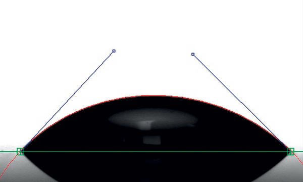
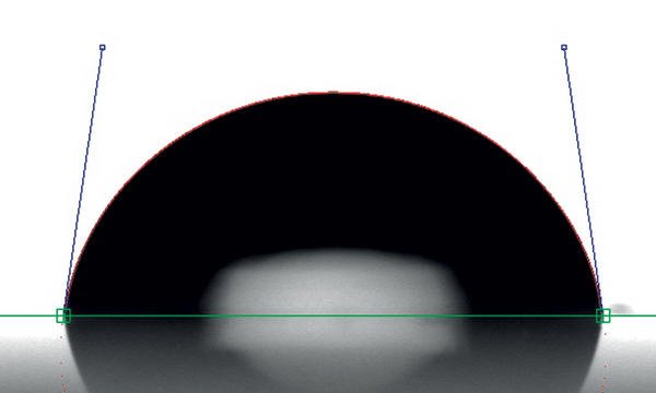
The non stick properties correlate with the surface tension of the nano coated stencil. The surface tension of solid materials is defined by the contact angle between a specific measurement solvent and the solid material. The contact angle is defined by the tangent touching the drop of the measurement liquid on the solid material (see figure 1). The value of the contact angle between liquid and solid material depends on the material specific surface tensions of the liquid and the solid phase. The measurement of the contact angle and the knowledge of the surface tension value of the measurement liquid allows calculating the surface tension of the solid material. Theory and experience tell us: A high contact angle between solid and liquid describe non stick properties (see figure 2). A low contact angle describes visa versa good wetting.
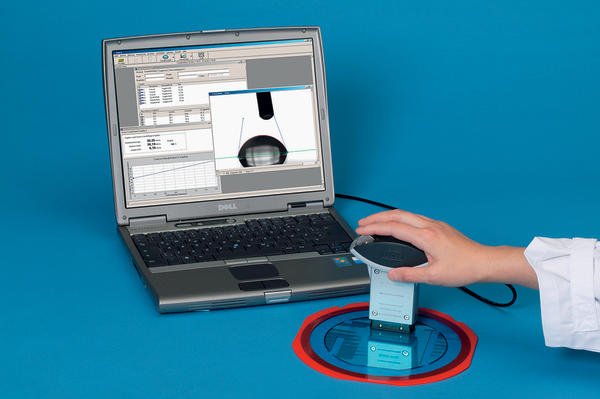
The classic sessile drop method is a good way to measure surface tension in quality assurance [1].The qualitative analysis of the contact angle is carried out in our days with computer controlled equipment with high accuracy and good reproducibility (see figure 3).
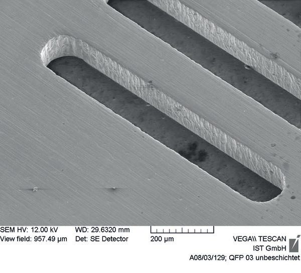
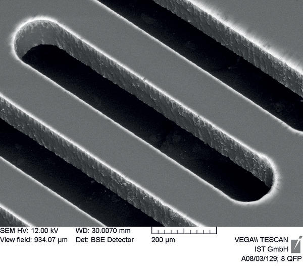
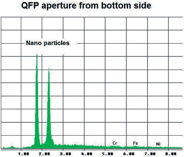
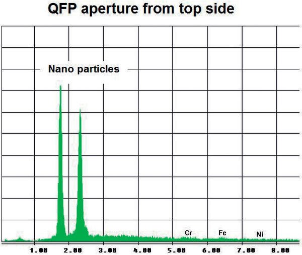
For fundamental research quality studies images from Scanning Electro-beam Microscope (SEM) are helpful tools to study homogeneity of the coating on the aperture walls as well on the bottom side. The comparison of different stencil technologies is shown in SEM (figure 4). QFP aperture of a laser cut stainless steel stencil and in figure 5 the same structure in laser cut stainless steel stencil with nano coating. With energy disperse X-Ray analysis it is possible to demonstrate the homogeneous distribution of the nano coating on the aperture walls (QFP 0.3 mm pitch.) Figure 6 shows the result from the bottom side and figure 7 from the top side.
Characteristics of nano coating
The nano coating from LaserJob is a reaction product of inorganic and organic materials. The chemical bond of durable inorganic compounds with non stick attributes of organic compounds are the core characteristics of the new material. Besides the significant improvement in solder paste release behaviour the new coating is particularly suitable for reducing stencil cleaning cycles and the amount of stencil cleaners. The stencils with nano coating provide really easy to clean products. This feature withstands more than 200 washing cycles with commercial available stencil cleaners! Significant economical use of stencil cleaners and productivity of stencil printers are commercial corner stones of LaserJob nano work stencils. Customers run now their productions with 50 prints without cleaning stencil bottom side and reduced failure rates.
Results from printing tests with different stencil types
The following studies carried out in the Institute for Manufacturing Automation and Production Systems, University Erlangen Nuremberg, together with studies conducted in the field summarises detailed the solder paste printing results.
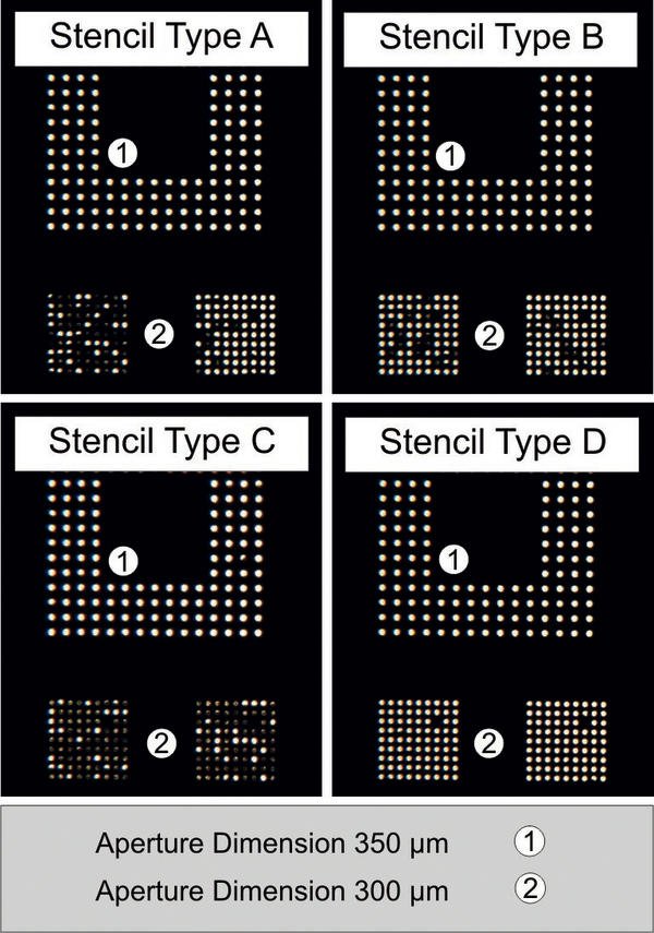
Following stencils with a thickness of 127 µm have been tested on a DEK printing machine. Solder paste: SAC type 3. Stencil bottom side was not cleaned, to rate the degree of pollution.
- Type A: Stainless steel laser cut with brushing treatment.
- Type B: Stainless steel laser cut with electrochemical treatment.
- Type C: Galvanic formed nickel stencil.
- Type D: Stainless steel laser cut with brushing treatment and nano coating.
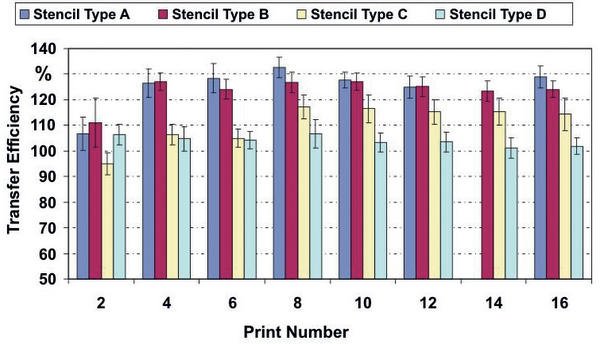
Already after the 5th print the type D stencil showed significant differences to the other stencil types. Figure 8 illustrates the transmitted light prints of the four stencil types. The test vehicle was a BGA structure with aperture diameters of 350 and 300 µm. The partial clocking of the 300 µm structures with stencils of type A, B, C also refers to low solder paste quantity transferred to the PCB in the 5th cycle. The nano coated stencil (type D) provides a 6 to 18 % higher solder paste transfer quantity compared to traditional stencils.
Another failure mode is the continuous increase of transferred solder paste volume due to stencil bottom side contamination with solder paste especially with fine pitch (pitch 300 to 400 µm) QFP structures. The solder paste residues do not longer allow a perfect contact between stencil bottom side and PCB. This leads to wet bridges on the PCB and later on to solder bridges in the assembled boards. Nano coated stencils provide in comparison to traditional stencils 6 to 18 % higher solder paste transfer relating to the nominal volume [2].
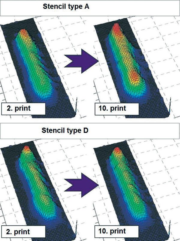
A more detailed expose is, to calculate the transfer efficiency in % of the nominal volume. In figure 9 it is evident, that state-of-the-art stencils will transfer without expensive and time consuming cleaning up to 130 % solder paste against the nominal volume! The increase of transferred solder paste quantities is not the only failure mode leading to bridging in the print process, additional broadening of the printed solder paste deposits takes place. This is a critical process with high negative influence on bridging. Figure 10 shows the broadening of solder paste deposits of 400 µm QFP structures depending from print cycle numbers.
Conclusion
The clocking of fine pitch apertures, as well as the contamination on the rear side of the stencil with solder paste can be reduced significantly by the use of nano coated stencils. The new nano coating stencil technology minimises the adhesion forces between solder paste and stencil. The measurement of contact angles on the rear sides of nano coated stencils show significant higher contact angles in comparison to traditional stencil technology. The unique physical properties of nano coated stencils overcome the risk of running under or over the designed solder paste quantity. Therefor failure modes open through too small paste volumes and bridges caused by too high solder volumes are reduced. The reliability of solder joints no longer depends on stencil cleaning cycles! Nano coated stencils have a high potential to optimise the solder paste printing process in technical and commercial aspects.
EPP Europe 438
zusammenfassung
Die Zuverlässigkeit von Lötverbindungen hängt auch von gleichmäßig übertragenen Lotpastenmengen während des Druckprozesses ab. Nanobeschichtete Schablonen mit Anti-Haft-Effekt optimieren das Auslöseverhalten der Paste. Sie können das Zusetzen feiner Aperturen sowie das Auftreten von Lotpastenresten auf der Schablonenunterseite bei zunehmender Druckanzahl erheblich reduzieren.
La fiabilité de l’assemblage par brasage dépend entre autres de l’uniformité d’application de la pâte à souder pendant l’impression. Les pochoirs à nano-revêtement avec effet anti-adhérent permettent d’optimiser l’activation de la pâte. Ils peuvent réduire considérablement l’apparition de petites ouvertures ainsi que la formation de résidus de pâte à souder sur la face inférieure du pochoir, parallèlement à un nombre croissant d’impressions.
L’affidabilità dei collegamenti saldati dipende anche dall’applicazione uniforme di quantità di pasta per saldare durante i processi di stampa. Gli stencil con nano-rivestimenti ad effetto anti adesivo ottimizzano il processo di distacco della pasta. Possono ridurre considerevolmente la formazione di piccole aperture e la produzione di residui di pasta di saldatura sul lato inferiore della maschera all’aumentare delle stampe.
References
[1] Contact angle measurements, http://www.kruss.de
[2] M. Rösch, D. Kozic, F. Feldmann: „Qualifizierung des Schablonendrucks unter Verwendung nanobeschichteter SMT-Druckschablonen“. Produktion von Leiterplatten und Systemen (PLUS), Eugen G. Leuze Verlag, 11/2007, Bad Saulgau, S. 2175–2179
Share:


