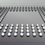
In electronics manufacturing, when there is a need to examine a printed circuit board rejected by a customer, an anomaly in production, or a prototype that has just been developed, manual X-ray (MXI) is a good choice. How long the inspection with any optional radiation penetration angle between tube and swiveling detector finally takes is not a decisive factor. Because it is separate from the production lines, it does not impact cycle times. However, if a one hundred percent examination of hidden solder joints is required, in-line X-ray systems are called for. Typical examples of components soldered in this way, where automatic optical inspection meets its limits, are QFNs (quad-flat no-leads package) and BGAs (ball grid array) as well as, e.g., the increasingly miniaturized LEDs.
Concept with parallel printed circuit board handling
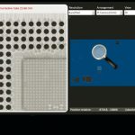
In-line X-ray systems must reliably point out defects that are invisible to the human eye; furthermore, they are constantly developing to keep pace with the rising demands for speed in electronics manufacturing. For example, today handling times as low as four seconds can be realized; as a result, up to three printed circuit boards can be present in the 3D AXI system at the same time. In order to keep the X-ray inspection from unnecessarily slowing down line beat, the faster 2D and 2.5D inspections can be combined with 3D inspections as required. 3D technology is applied where it is most efficient.
Results without interfering structures
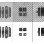
It is helpful for the inspection to gain slice images from volume information. Both horizontal and vertical slices can be extracted. Because of the extremely complex overlapping, especially with printed circuit boards populated on both sides, this capability is essential. In this case, with a 3D reconstruction, all significant features can be made sharply visible in clear slice images – even for shadowing by components or on multi-layer boards. While details of the back side are always seen in 2D X-ray images, the 3D slice image eliminates all such interfering structures. This greatly simplifies inspection program generation and enables effective false call prevention. For improved verification, planar computed tomography of a 3D AXI system can be applied to generate partial or complete volumes of the inspected solder joint, which can then be tilted, rotated and zoomed on the monitor.
3D AXI on the example of LEDs
When LEDs are examined more closely, it is immediately apparent that a 3D AOI on its own is not enough to guarantee high quality in the final product. In-line X-ray provides the ideal means, especially to precisely inspect the associated hidden solder joints. Innumerable application possibilities from interior lighting, streetlights, and displays are open for LEDs, and for industrial designers, a wide latitude in implementing their lighting ideas. The automotive branch in particular was quick to recognize the potential of this technology, which has long since established itself as the standard in vehicle lights, flashers, and headlights. Its inherent advantages include a long service life, high light yields, and low energy consumption.
Heat dissipation is a decisive quality feature
LEDs emit not only light, but heat as well. Quick dissipation of this heat is critical for their longevity. The electronics association IPC has not specified any standards for heat dissipation in their acceptance criteria. These standards state only that for components with connections to heat sinks on their bottom sides, the criteria for the hidden areas of the solder joints on the thermal level must be determined by agreement between user and manufacturer. For the heat transition layer, these criteria depend on process and design, whereby the component manufacturer‘s application notes, solder coverage, pores, solder height, etc., must be taken into account. Formation of pores and bubbles in the thermal layer when these component types are soldered is normal. However, hollow spaces in the solder joints (voids) in particular can prevent optimal dissipation of heat from chips and semiconductor component barrier layers. The life span (operating hours), wavelength (color), and even the light yield (brightness) of the LEDs are strongly dependent on the barrier layer temperature.
High efficiency under strict requirements
Especially in the automotive industry, manufacture and quality control of printed circuit boards assembled with LEDs are often sourced to EMS providers (Electronic Manufacturing Services). They must meet the strict requirements of their ordering customers and at the same time, be as efficient as possible to stay competitive. Here, brand manufacturers specify very precisely just how high a percentage of voids in solder joints is acceptable. Process ovens with vacuum chambers and other means can help prevent voids. Those that do form can be very clearly identified with cutting-edge 3D X-ray. While a flexibly applicable manual system is adequate for random inspections, one hundred percent, fully automatic inspection is performed by a system in the production line. This way, voids can be completely recorded and analyzed, even while hidden from an outside view.
X-ray and optical inspection supplement each other
Nevertheless, the importance of 3D AOI in inspecting LEDs is by no means overshadowed. Especially in automotive applications, there are very specific requirements for the positioning and alignment of the components. Detecting defects such as minimum non-coplanarity of the ever smaller LED components depends on reliable measurement values. To support the absolute precision and repeatability of 3D AOI, an exactly manufactured height gauge – measured with high precision instruments by a specialized laboratory and certified – can be used as a target standard. Tilted components can be detected with 3D AOI very well; precise measurements are also achieved for rotations and X/Y offset. Thus, the AOI also makes a decisive contribution to quality assurance.
Different inspection methods in the optimized process
3D AOI and 3D AXI have been optimally incorporated in a single machine for many years now. Printed circuit boards move quickly and nearly simultaneously between the two inspection sections and the combination of different inspection methods can be versatilely adjusted to suit the task. Furthermore, a networked evaluation including results from a solder paste inspection (3D SPI) is an effective adjunct to process improvement. Taken as a whole, assembly inspection in electronics manufacture is a prime example of successfully implemented Industry 4.0. Intelligent 3D SPI systems communicate with paste printers and placers; result data from 3D SPI, 3D AOI, 3D AXI and 3D MXI can be quickly retrieved at connected verification stations – even for several production lines – and statistical process control facilitates an overview of defect distributions within set tolerance limits. Analyzing the data from detected false calls and real defects delivers valuable knowledge of whether changes in the process are needed or, e.g., if one component type is especially prone to defects. In addition, with the high amount of information the inspection systems provide for each individual assembly, cross references can be drawn throughout the entire production.
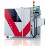
 Viscom AG, from Hanover, Germany, has developed an extremely fast printed circuit board transport especially for in-line X-ray inspection.
Source: Viscom AG
Zusammenfassung Résumé Zusammenfassung russisch
Immer mehr Elektronikhersteller wollen für verdeckte Lötstellen Inline-Röntgensysteme (AXI) einsetzen. Dabei geht es um schnelle Prozesse in Verbindung mit erstklassiger 3D-Bildqualität. Ein Beispiel ist die sichere Erkennung von Voids, welche bei der Herstellung von LEDs und anderen Anwendungen benötigt wird.
De plus en plus de fabricants de produits électroniques souhaitent utiliser des systèmes à rayons X en ligne (AXI) pour les joints de soudure dissimulés. Cela implique des processus rapides associés à une qualité d‘image 3D de première classe. Un exemple est la détection sécurisée des vides nécessaires dans la fabrication de LED et d’autres applications.
Всё больше производителей электроники хотят использовать линейные системы рентгенографии (AXI) для закрытых точек пайки. При этом речь идет о быстрых процессах в сочетании с первоклассным качеством 3D-изображения. Примером является надежное распознавание пустот, которое требуется при производстве светодиодов и в других задачах.
