Fine-feature solder paste printing for passive component sizes, from 01005 (0.4 mm x 0.2 mm) and now down to 008004 (0.25 x 0.125 mm), has become more challenging in SiP assembly. Due to small stencil aperture designs, finer powder size solder pastes, typically type 5 (15 – 25 μm), type 6 (5 – 15 μm), and type 7 (2 – 11 μm), are used for these applications. Since more components are being packed into a SiP, the rheology of the solder paste is an important attribute, as the gap between neighboring pads can be as close as 50 μm. Solder paste with minimal slump behavior will be required to minimize bridging in such designs. Consistency in solder paste printing transfer efficiency, stencil life, good wetting, graping resistance, and minimal voiding are other key attributes of solder paste for SiP assembly as well.
Desire for zero failures
As the trend toward miniaturization in SiP applications continues, from current 01005 components going down to 008004 (0201 m) or even 0050025 for next generation packages, the printing performance of solder paste becomes critical. The conventional SMT solder paste printing process using type 3 or type 4 powder size has evolved into a more complicated printing process for SiP, using types 5, 6, or even 7 powder size, with much smaller stencil apertures, thinner stencils, and more stringent requirements for allowed paste deposit variability.
SiP, and similar forms of heterogeneous integration, are now being adopted in complex automotive systems where space is a premium. For many years there was confusion about the appropriate reliability testing for these packages, but the recent issuing of AEC-Q104 Failure Mechanism Based Stress Test Qualification for Multichip Modules (MCM) in Automotive Applications makes it clear that SiP can be covered within the main AEC-Q100 spec, SiP…. can be qualified within the scope of AEC-Q100 per Section 2.1.
The desirability of zero failures for complex systems, ultimately driven by the desire for increased safety, and most especially by ISO-26262:2018 (road vehicles: functional safety) has meant a dual approach for automotive system design engineers: design for reliability at the ppb level, and (unfortunately from a cost perspective) build-in redundancy for mission-critical subsystems. Consistent, low-voiding solder joints lead to enhanced reliability. It is the SiP assemblers’ task to create reliable miniature solder joints, even when dealing with fine-pitch solder paste at quantities of tonnes per year.
In addition to printing a smaller and thinner solder paste deposit, the gap between neighboring pads is smaller, too. Some customers are already looking at a gap of 50 μm between pads. In order to achieve good and consistent printing performance under such challenging conditions, besides having good printer setup and appropriate stencil technology2) 3), the choice of correct powder size, flux system, rheology, and slump behavior of solder pastes is key.
Solder powder
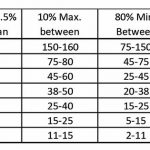
Powder size is classified by type according to IPC J-STD-005A. The table outlines the different solder powder sizes available in the electronics and semiconductor industries. Although types 3 – 5 are increasingly in use for SMT, some OSATs (outsourced semiconductor assembly and test companies) and others are already using powder size type 6 for SiP with 01005 chips; for next generation packages with 008004 chips, both types 6 and 7 powder sizes are being considered.
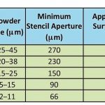
It is a general industry guideline that in order to achieve consistent solder paste printing performance, it is important to choose the correct powder size so that a minimum of 5 – 6 solder particles (the large particle size of the range) can be maintained across the aperture. According to this rule, there is a recommended minimum stencil aperture for each powder type.
Another concern when choosing a smaller powder size is the increase in the powder surface area. As shown in the table, when powder size decreases from type 3 to type 7, the powder surface area increases significantly. This increased powder surface area will require more flux activation, or flux with a better oxidation barrier to protect the powder from surface oxidation2). Hence, it is important to both choose a correctly formulated flux that works with finer powder, as well as a solder powder with a low oxide level. These factors will enhance the stability of the fine-pitch solder paste in terms of shelf life, stencil life, and wetting or solderability performance. Excessive activator levels can also destabilize the paste, so flux formulation is complex.
Flux system
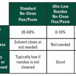
Different types of flux systems are typically available: water-soluble flux, standard no-clean flux, and more recently, the ultra-low residue (ULR) no-clean flux have seen widespread use, especially in semiconductor assembly applications4).
Currently, most SiP applications use the water-soluble flux system, where the residue is cleaned away using water after reflow, followed by the drying and overmolding steps. As the miniaturization trend continues, some SiP applications will soon reach a point where effective cleaning with a very tight gap and standoff becomes challenging, and using an ultra-low residue no-clean paste will be necessary. This new class of solder paste enables all cleaning and chemicals process costs to be eliminated, while reducing both component warpage and cycle time.
Paste rheology
Decreasing the powder size of the solder paste increases the viscosity, though, since the flux vehicle itself is thixotropic. The paste used in stencil printing is a shear-thinning thixotropic material5) with a low yield stress, the rheology being governed by both the flux system and the solder powder. The paste rheology controls a variety of factors: paste aperture filling ability, transfer efficiency of paste from stencil onto substrate, and the shape of the paste deposit after printing. These are keys for good printing performance of a solder paste.
Paste slump
The term “slump” describes an x-y direction expansion of the solder paste deposit caused by gravity. A yield stress in the paste can prevent slump. A metal load that is too high can give the paste a very high yield stress and prevent the paste from filling and releasing from stencil apertures; therefore, optimizing the metal load for the printing process is important and is driven by several factors.
Paste stencil life
A solder paste with long stencil life is important to reduce print-to-print variability over time. Typically, a stencil life of at least 4 to 8 hours will be required for a high-volume manufacturing environment.
Printing experiment
Several combinations of paste, tooling setup, and stencil aperture sizes were investigated, together with three solder paste specimens featuring different flux chemistries and different powder sizes. Also, a board support system of pallet and vacuum support were compared to investigate whether the use of a pallet alone could allow the printing process to achieve a comparable consistency. Finally, laser-cut and electroformed stencils were compared by printing different apertures sizes.
Test vehicle
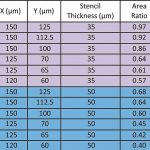
A test vehicle was specially designed to mimic a typical substrate size of 237 mm in length, 62 mm in width, and 0.5 mm thick. There are two arrays of pads on the test vehicle. Each row has different pad sizes: 150 μm x 125 μm on row 1; 150 μm x 100 μm on row 2, and 150 μm x 112.5 μm on row 3. Each column has a different gap distance between pads, i.e., 50 μm, 80 μm, 100 μm, 130 μm, and 150 μm. Pads are arranged in horizontal and vertical positions such that different squeegee wiping directions could be simulated. The pad surface finishing is NiAu (ENIG, electroless nickel immersion gold ) and are non-solder mask defined (NSMD). The test vehicle also consists of 01005 pads, but it is not the focus.
Paste specimens
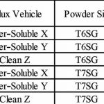
Three flux vehicles were chosen in this printing test: two water-soluble fluxes and one no-clean flux. These three fluxes were mixed with type 6 and 7 powders. As finer powders yield higher viscosity, a slight tweak in the metal load for type 7 pastes is needed to reduce the viscosity to about the same viscosity as the type 6 solder pastes.
Stencil design
Three stencils were prepared for this study: one 50 μm-thick laser-cut stencil and two electroformed stencils with thicknesses of 35 μm and 50 μm. The laser cut stencil has a 1-to-1 opening with the pad size on the test vehicle, while the left array of the electroformed stencil follows a 1-to-1 opening, and the right array has a smaller aperture. The two electroformed stencils have the same aperture designs but only differ in the stencil thicknesses.
Equipment and tooling setup
- DEK Horizon printer
- Koh Young SPI machine
- 12 “ squeegee at 60 ° wiping angle
- Vacuum support
- Carrier pallet
Printing parameters
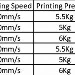
Print speed was fixed in all experiments while the squeegee pressure was adjusted so that minimum pressure was used in each experiment, i.e., enough pressure to just wipe the stencil surface clean, see table. A minimum pressure is crucial in achieving consistent prints as excessive pressure could cause movement of the printing surface during the squeegee stroke. Cleaning frequency was set to three pieces, with a cleaning mode of wipe/vacuum/dry (W/V/D).
Bridging between pads
The comparison demonstrates a clear difference between tooling combinations. By using for the board support a carrier pallet, no bridging was observed down to an 80 μm gap distance when using a laser cut stencil. By using a vacuum support, the laser-cut stencil was able to achieve non-bridging at the 50 μm gap distance column. This suggests that the vacuum support provides a much better functionality with minimal gap between the stencil and PCB during printing.
However, with electroformed stencils, one array prints encountered bridging. The amount of bridging increased from column 1 (50 μm gap) to column 5 (150 μm gap). The increased transfer efficiency of the electroformed stencil is most likely the cause for this distinct difference in print performance. The other array with reduced apertures did not give any bridging.
Comparison of solder pastes
On the other array, the aspect ratio ranges from 0.40 to 0.45 only for a 50 μm thick stencil. However, a consistent print is still achievable for these pads. Comparing the deposit volume of the three pastes with different aspect ratios shows: paste C ranks the best among the three pastes; paste A ranks second; and paste B is third. Paste B has a tighter distribution compared to paste A and paste C; however, it has many more insufficient compared to the other two pastes. The rheology plays a big role in printing ultra-fine apertures, and good printability is achievable with both water-soluble and no-clean flux chemistries.
The 35 μm thickness stencil gave a higher aspect ratio, hence it was believed that the thinner stencil could yield better printings over the 50 μm thick stencil. The aspect ratio improved from a range of 0.40 – 0.45 to 0.57 – 0.64. The improvement was obvious by using paste sample C. The printing results of T6 and T7 pastes show that the standard deviation of T7 prints is smaller, so it has a lower variation. However, it was also observed that more bridges were seen.
Process capability
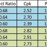
Cp, Cpk, and Ppk were calculated using Minitab software. The reference specification limit used was 40 % to 150 % to compare the paste performance. Both vacuum support and carrier pallet are capable setups, as the table reveals; however, vacuum support has a greater consistency as the Cpk and Ppk values are larger. The process capability of all pastes can be seen in the table, using various pad sizes and stencil thicknesses. The combinations of pad size and stencil thickness were represented as their respective aspect ratio.
Reflow and test vehicle
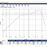
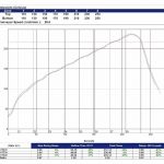
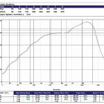
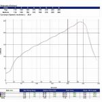
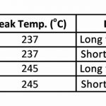
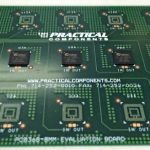
Reflow testing was done on one of the water-washable pastes that is being used in a high volume SiP application to study the void performance with different reflow profiles in air. The Practical Components test board was used, with pad and stencil apertures both of 180 μm circles. The thickness of the stencil was 75 μm. Four different profiles were tested as shown in the diagrams. The actual profiles were recorded.
Results and conclusions
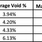
The results are summarized in table and figure. For this particular water-soluble solder paste, the voiding is affected by different profiles. The long profile with soak zone shows a lower void %. The relationship between the void performance and reflow profile should be adequately characterized for each solder paste, as different solder pastes may work best with different temperature profiles.
In order to achieve consistently good fine-feature printing performance for SiP applications, solder paste attributes, i.e., powder size, flux system, rheology, slump behavior, and stencil life, are important and need to be taken into consideration. Solder paste with suitable rheology, mixed with the correct powder size and flux, should be evaluated and selected accordingly. The suitable stencil technology, design, and thickness, coupled with an appropriate board support system, are also keys for consistently good solder paste transfer efficiency. Reflow profiles need to be properly characterized in order to minimize voiding for different solder pastes.
SMTconnect, Booth 5-310
Acknowledgement
Special thanks to Indium Corporation’s Suzhou Simulation Lab team – Ms. Wisdom Qu, Dr. Fiona Chen, and Leon Rao – for their help and support in performing the solder paste printing tests in their lab. First presented at IWLPC, October 2016, San Jose, California.
References
- Lim, Thum and Mackie: Meeting Solder Paste Printing Challenges for SiP in ‘Smart’ IoT Devices, Chip Scale Review magazine, Jul-Aug 2016.
- Ed Briggs: Meeting Future Stencil Printing Challenges with Ultrafine Powder Solder Pastes, International Conference on Soldering and Reliability, Toronto, Canada, May 2014.
- Rita Mohanty Ph.D., S. Manian Ramkumar Ph.D., CEMA, Chris Anglin, Toshitake Oda: Effect of Nano-Coated Stencil on 01005 Printing, APEX 2011.
- Sze Pei Lim, Maria Durham, A. Mackie: No Clean Material For Advance Packaging Assembly, Semicon China, Feb 2016.
- Kravcik and Vehec: Study of the Rheological Behavior of Solder Pastes, Proc. Scientific Conference of Young Researchers 2010, FEI TU of Kovice.
Zusammenfassung
In der Automobilelektronik finden sich mit steigender Tendenz SiPs in den vielen Helfersystemen für die Fahrer – insbesondere in Systemen für die Advanced Automated Driver Assistance (ADAS). Doch stellen die SiP-Bausteine deutlich höhere Anforderungen an den Fertigungsprozess der Baugruppen, insbesondere an Lotpaste, Flussmittelchemie und Reflow.
Résumé
Dans l‘électronique automobile, les SiP se retrouvent de plus en plus dans les nombreux systèmes d‘assistance à la conduite, en particulier dans les systèmes d‘aide à la conduite automatique avancée (ADAS). Cependant, les composants SiP imposent une demande plus importante au processus de fabrication des assemblages, en particulier en ce qui concerne la pâte à souder, la chimie des flux et la refusion.
Резюме
В автомобильной электронике все чаще применяются корпуса с однорядным расположением выводов (SiP). В частности, это касается множества систем помощи водителю, например Advanced Automated Driver Assistance (ADAS). Однако при производстве к узлам SiP предъявляются более высокие требования. Речь идет о паяльной пасте, флюсе и системах пайки оплавлением.
