

Implementing the appropriate materials and provisions that take advantage of determinate laws of physics, it is possible to produce what is normally called a “laser beam”, which is substantially a light or a well-defined electromagnetic wave.
Monochromatic and collimated
However, this is not a common electromagnetic wave, but rather radiation which has the capability to create a “coherent” flow, in terms of space as well as time.
Two important properties are the result of this capability:
- The first is being “monochromatic”, therefore characterized by a limited set of wavelengths which, depending on the type of materials used, can range from infrared to ultraviolet.
- The second is being “collimated”, therefore composed of a set of parallel and unidirectional sub elements.
In particular, the latter of these two properties, collimation, enables the laser to convey energy with a density (energy/surface) much higher than a standard light source. In other words, a laser can be considered as a source of energy which can be conveyed to a target (very small and defined areas) without making contact (contactless).
Choosing the appropriate wavelength of the laser source allows to optimize the laser beam according to the process and the materials involved, in order to achieve the best transmission and power absorption by the target. From the output of the source, the laser beam can be conveyed via optical fibers, or through a system of fixed or movable mirrors driven by galvanometers, in order to deflect the beam where necessary. A fundamental component of a laser system are the optics, whose task it is to focus the laser spot in the desired manner and shape.
PCBA assembly technologies
Over the course of the last decades, the evolution of electronic component and electronic board assembly technologies has seen a gradual decrease of Through Hole Technology (THT) components, that is those having leads that are inserted through a hole in the printed circuit, in favor of surface mounted components (SMD). The advantages of SMD technology are widely noted, but they are not relevant in the context of this article.
It is a fact that, even though the complete elimination of THT technology was predicted, it never happened. Anybody who assembles electronic boards is aware that, to different extents, it will be necessary to face the problem of mounting and soldering some THT components onto boards (sometimes only connectors). Above all, it has to be done quickly (especially for high-volume productions) and accurately, making sure not to damage what is already on the board. Ensuring the quality of the product is also important, which until that moment, has been involved in less critical, high-yield assembly processes.
Recently it has become common that products are designed and engineered to include one or more electronic boards, which are placed in plastic or resin casings (composite casting). In this case, the junction between the electronics and composite item is often done with metal mounting tabs, which ensure the connection between the parts, and are soldered in the same way as the THT leads. These linking elements often have significant cross-sections, since they carry high-intensity current.
Laser and selective soldering for electronics
The challenges faced in electronic board manufacturing are becoming increasingly difficult. First of all, volumes, which can reach high numbers in some industries, can impel incessant cycle times. There are also the quality targets, that require not only high process yields, but also the production of a final product able to withstand mechanical, thermal and electrical stresses over a long-life cycle. In addition, there are layout, weight and design requirements which mandate that the electronics be inserted into complex positions and containers, which standard soldering systems have poor ability to handle. Finally, to withstand the impact of all these technological challenges while reducing costs, it becomes strategic to adopt machinery and production technologies with a high level of automation.
In this scenario, it is easy to conclude that laser has some intrinsic characteristics that make it a very interesting technology to use as the basis for a selective soldering system to be deployed in the finishing phase of PCBA.
In particular, there are some fundamental considerations:
- No contact on the solder joint is required.
- The agility to easily access boards with accessibility issues and problems caused by the close proximity of adjacent components.
- The possibility to operate on boards having the bottom side facing upwards (which is not uncommon in some automated lines).
- The possibility to modulate the amount of energy and to vary the area of distribution depending on the specific joint to be soldered.
- The capability to implement a highly reliable and repeatable process.
- The flexibility to adapt to changing production needs without any additional tools or equipment.
These are only few of the reasons in favor of its application.
Laser and selective soldering: a constantly evolving technology
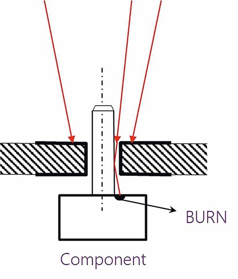
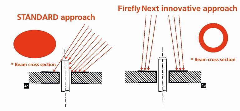
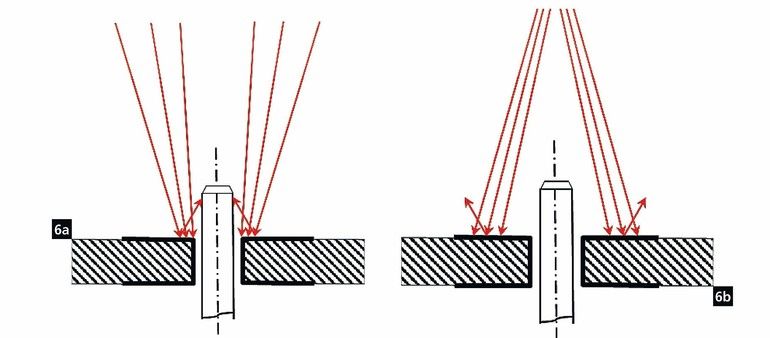
In the past, using a laser beam coming from a completely vertical angle with respect to the solder joint had already been excluded from the approach of laser selective soldering, due to a series of contraindications. In particular, it is impossible to eliminate the portion of the laser beam which, by force of circumstance, passes through the narrow space between the component lead and the walls of the hole and hits, and consequently damages, the component mounted on the opposite side. For this reason, the standard approach to this type of process was to use an angled conical laser beam, which considerably reduced the amount of radiation which could pass through the hole. The angled conical laser beam, combined with the possibility to modify the distance between the laser source and the target, also provided the capability to change the radiated surface, thus adjusting the process parameters.
Despite the application of sophisticated control technologies, such as a laser distance sensor between the power source and the board to compensate for board warpage, a pyrometer to obtain feedback on the trend of the thermal profile, and a wire feeder equipped with a sensor to ensure the repeatability of the correct distribution of the filler material, the result of this approach was not exempt from basic problems. In particular, it was not possible to exclude damage to the component. Although minimized, there could be instances where the laser radiation could still pass through the hole, reaching the component mounted on the opposite side. A portion of the laser beam aimed at the lead of the component could be reflected and reach the pad edge, damaging both the PCB and the adjacent solder mask.
The analysis of the results, combined with in-field experience, identified the issues of this standard approach, and pointed to two features of the solution: on one hand, the angle of the laser beam (causing reflection on the lead), and on the other, the shape of its cross section, its full-section oval footprint (main cause of energy “infiltration” through the hole).
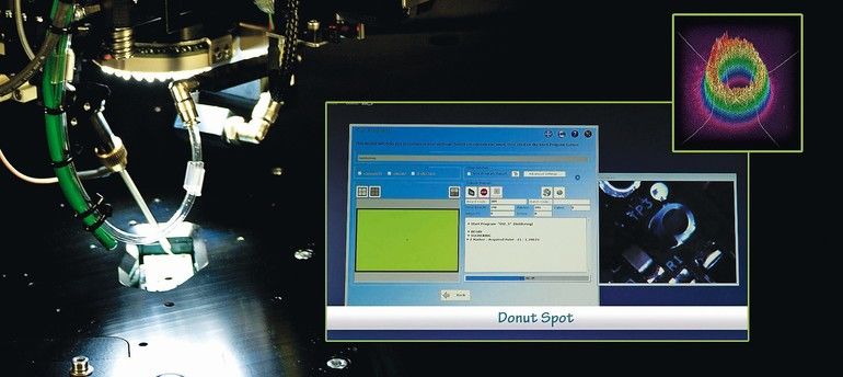
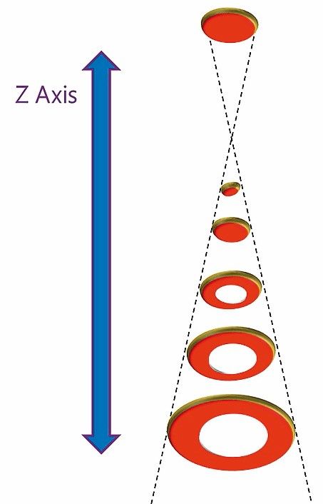
For this reason, the study was focused on the optical system, with the goal of obtaining a “hollow” beam (“donut-shaped”), which would eliminate the passage through the hole and enable a return to a vertical position of the laser beam over the target. In essence, the shape of the laser beam would be optimized, in order to be able to transmit energy exclusively to the copper pad and only from a vertical direction, thus reducing the possibility of unwanted reflections on the lead, while preventing any possible radiation going through the hole. Regarding the laser beam direction, it should be noted that its shape, defined by the optics and created to fit the standard pads and holes of printed circuit boards, is not convergent towards the pad, but divergent.
By changing the distance between the laser source and the target, the characteristics of the laser beam allow the external and internal diameters of the two circumferences to be modified, in order to achieve optimum energy transmission to the targeted pad.
From a practical point of view, instead of maintaining the architecture of the standard approach, which implemented each element of the soldering system separately, the new solution combines all of them in a single unit with a shared optical path, allowing for a better balance and calibration of the entire system. In fact, in Seica’s innovative solution, the laser source, camera and pyrometer are all positioned on the same path, minimizing variances and preventing misalignments.
A winning choice
Today’s industry needs dedicated solutions, specific competences, optimisation of processes and investments. An automated, laser-based selective soldering system offers a solution for electronics manufacturing needs by virtue of the integral characteristics of the solution:
- Laser technology allows for no-contact soldering especially in situations where there is limited access, for whatever reason (component density, pad size, product casing, etc.)
- Complete automation ensures that soldering is constant and repetitive, components are soldered correctly without undesirable thermal stress, and the entire process has total traceability.
- The laser soldering process is clean, which eliminates the need to clean, therefore subsequently handle, the processed boards, and power consumption is extremely low compared to other types of soldering technologies.
- The process is totally waste-free and highly flexible for all applications.
Selective soldering is a well-known and consolidated technology, used to solve many issues concerning the soldering of THT components. Among the existing solutions, the one which uses laser as the energy source has reached high levels of applicability and repeatability, resulting in accurate and reliable systems, perfectly capable of meeting the high qualitative demands of the electronics manufacturing industry. The scalability of systems, combined with the possibility of integration into custom automated lines, provide an additional level of flexibility to best meet factory requirements.
Seica S.p.A.
Via Kennedy, 24
10019 Strambino (TO) Italy
Tel.: +39 01256368 11
E-Mail: seica@seica.com
Website: www.seica.com
 Source: Seica S.p.A.
Alberto Ghirelli
Pre-Sales & Product Development, Seica Strambino.
Selektivlötsysteme, die den Laser als Energiequelle nutzen, erreichen ein bedeutendes Maß an Anwendbarkeit sowie Wiederholbarkeit und sind so perfekt in der Lage, die hohen qualitativen Anforderungen der Elektronikfertigungsindustrie zu erfüllen.
Les systèmes de soudure sélective utilisant le laser comme source d‘énergie, atteignent un niveau élevé en matière d’applicabilité et de répétabilité et sont parfaitement en mesure de satisfaire les exigences qualitatives élevées de l’industrie de l’électronique.
Селективные системы пайки с использованием лазера в качестве источника энергии применяются все чаще и обеспечивают все более высокий уровень воспроизводимости, в полной мере удовлетворяя высоким требованиям к качеству, предъявляемым в электронной промышленности.


