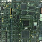
Referring to an electronic board, the reverse engineering process consists of:
- Netlist regeneration;
- XY target coordinates: test point/pad/pin/via center;
- Bill of Materials (BOM) regeneration;
- PCB CAD file regeneration;
- Schematic diagrams regeneration.
Why use reverse engineering
In military aerospace and partially in telecommunication, railway and electronic manufacturing industries, there are pieces of equipment with a long lifecycle: up to 40 years or more. Over this time, electronics can stop working or the electronic manufacturer can even leave the business. When spare parts are not available or very expensive, it is then mandatory to repair faulty boards.
If the electronic board is very old, the manufacturing data or schematics could have been lost. This means that repairing a board can be a very long, frustrating and expensive task, if data isn’t available. In this case, reverse engineering can be the only solution.
Accordingly, one of the main reasons for reverse engineering is to build spares in similar environments where the manufacturer itself has lost the board data or when it does not exist anymore. This process also allows the user to repair, copy, clone, test or redesign a PCB module, despite the CAD data not being available.
Methods used for reverse engineering
Mainly, two different methods can be used to rebuild the netlist of a board.
Optical method: Easy with simple double-side PCBs. In the past, this was the only method available. In case of multi-layer boards, to rebuild tracks and netlist visually, highly specialized companies would remove each layer from the PCB. This process was very time consuming and expensive.
Electrical method: Between two points, a short means that these belong to the same net. Theoretically, a continuity test between each point and all the others, provides all the information concerning the netlist. Nevertheless, the total continuity test is very high: 500,000 tests for a board with 1000 pins. Which isn’t easy for a human. The electrical method can be divided into two other categories:
- Capacitive measurement, which is almost obsolete and unused.
- Dynamic impedance measurement, which acquires the net signature of an analog dipole.
Automatizing reverse engineering
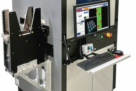
This long process can be automized with the Pilot V8 Next Series tester by Seica. The PCB accessibility on both sides is a preliminary and mandatory condition to fully rebuild the netlist because this is the only way to learn the connections between SMT components on opposite sides. The vertical architecture is the best mechanical damping because board vibrations are not increased by the force of gravity. Sophisticated but easy-to-use algorithms drastically decrease the total amount of tests, reducing the total reverse time and costs. The rebuilt data is ready to use to generate a test program by automatic procedures.
Board analysis
Thanks to multiple inspection and analysis techniques, the Viva software may operate both on mounted and bare boards. The reverse engineering can have a destructive or a non-destructive approach. The first method will destroy the device during the test procedure, while the non-destructive process retains full functionality of the device under test after the analysis. The Pilot V8 Next Series tester features a non-destructive method, although the following exceptions must be taken into account and solved:
- Microchips with BGA packages with the pins below the component, because it is necessary to expose the components with no accessibility.
- Protective coating that is a thin polymeric film applied to a printed circuit board (PCB).
The result of the netlist auto-learning procedure depends on the real accessibility of the probes on the test points. It is possible to analyze the following types of electronic boards:
- Bare board: this condition provides a complete and reliable learning of all the netlists on the PCB. Moreover, the check of the data learned is relatively easy and fast.
- Partially mounted board: to enhance the accessibility and minimize the subsequent manual operations, it is recommended to remove those components which prevent the access to some pads.
- Fully assembled board: in this case, the limited accessibility to the pads may require the execution of manual netlist learning using the dedicated tools available in the Viva software.
Board layout learning
At this point, with the so-called “net-oriented test methods”, it is possible to extract the netlist using only a golden board.
Autolearning: Dual side board digitalizing
The CCD color cameras, available on each side of a Pilot V8 flying prober, digitalize two detailed images of the top and bottom sides of the board. The company has developed several manual and automatic routines that identify the XY location coordinates using the built-in AOI system. There are four modes for auto-learning all the points and components of a board: manual, automatic, connector and component. This technique reproduces the full layout and it is useful for data processing and analysis, either online (auto-learn) in the system or offline (digitizer) on a remote PC.
Netlist learning
The first step is to manually identify at least one GND point. Similarly, the user can determine the VCC point if it is useful for the netlist analysis. Once the user has classified the GND signal, the “netlist learning” process on the flying prober can start with the Fnode macro.
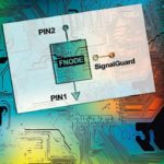
The company employs a proprietary dynamic impedance measurement method designated as Fnode, which acquires the net signature of an analog dipole. This powerful test method is used to measure the dynamic impedance of an unknown dipole to recognize and separate all the nets of a mounted board. From that, it creates a suitable number of continuity tests.
Since each dipole of the UUT is unknown, an “auto-learn” of the golden board is used to acquire the behavior of the dipole over a broad frequency range.
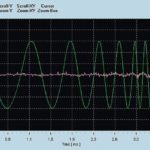
The typical input signal amplitude is 0.2 V to be below the P-N transition threshold and to avoid nonlinear distortions, as well as, to avoid guarding (electrically isolating the net environment to perform an individual measurement on a single component). The Fnode measures the current which flows into the dipole and, in each case, the amplitude and the phase for each net is stored by the test program. The Fnode is a purely passive measurement procedure, with no power on the UUT.
The advantages of Fnode are easily summarized:
- It does not need any CAD data and no manual debug is necessary.
- The auto-learn process is fully automatic and creates a full shorts test with higher fault coverage than the traditional adjacency test. Moreover, many in-circuit measurements can be avoided without decreasing test coverage.
This procedure utilizes a DSP-based (Digital Signal Processor) multi-function instrument, which digitizes the generated and measured signals. The acquired data enable the almost simultaneous execution of multiple, high-speed tests, because the test models are “hardware-emulated”, substantially increasing the test throughput.
Continuity macro
If two or more nets have the same current signature, the next step is to execute the continuity test. The main goal of the continuity macro, optimized to work in sets of 1000 tests each, is to group the test pads belonging to the same net. This procedure is also capable of detecting as separate nets the signals connected to low impedance (e.g. inductors, resistances at 0 Ohm…) when belonging to two-pin components regularly declared in the graphic environment edit board of the Viva software.
Power monitor
At this point, it is necessary to acquire the signatures/functions of the digital components. Once the GND and VCC inputs have been identified, the UUT is powered on to execute the Power Monitor (PWMON). It is possible to measure the current needed to produce logic 0 or logic 1 on each node (input pin of a digital component). This way, the threshold is learned, and the system can recognize a possible error on a net. Using this method, a “golden board” is not necessary but strongly recommended.
The advantages of PWMON are summarized as follows:
- It is a vector less method to test ICs in a powered-up condition.
- It can be generated without CAD data.
- It does not require manual operations, since it is a fully automatic procedure and it is independent of the UUT initialization conditions (when the UUT is powered on).
Data verification
When the netlist learning procedure has been completed, it is possible to check the results, to analyze and verify the data. The company provides tools that generate a list of points, connectors and components, electrically isolated from the netlist (capacitors, resistances, …).
Test program creation
Once the netlist learning procedure has been completed, along with the possible manual connection of some nets, the task carried out may be employed to create a test program for repair activity purposes, and/or create the data to be employed to rebuild the board schematics.
Schematics creation (from Viva to Elgris)
The final step of the reverse engineering is to export data from Viva to Elgris E-studio in order to generate the schematics in .PDF format.
Conclusion
As a result, the company’s flying probers are not only flexible tools used to test boards. They can also be very useful in reverse engineering, both for testing and deducing engineering decision-making based on end products of which little knowledge about the procedures involved in the original production is available. The flying prober is equipped with specific software and hardware characteristics and algorithms, which enable the generation of a comprehensive test program without CAD data or a bill of materials. The unique software tools and mechanical capabilities of the flying prober allow the facilities for assigning test points and entering component information, so that a full data package can be generated for future production builds, field repairs, or contractual obligations.
productronica, Booth A1-445, A3-337, B3-570
Giada Ferraro graduated with honors in Electronic Engineering at the Politecnico of Turin in 2017.
She started her career at Seica S.p.A. (Italy) in 2017 as an application engineer, working especially in the functional test environment.
After one year of experience, she moved to the new Pre-Sales and Product Development group.
Giada and her colleagues cooperate with internal departments to fulfill the terms of the contract between Seica and the customer and investigate the industry trends to upgrade the brand knowledge.
Zusammenfassung
Die im Artikel vorgestellten Flying-Probe-Systeme sind nicht nur flexible Werkzeuge zum Testen von Boards. Sie können auch im Reverse Engineering sehr nützlich sein, sowohl für die Prüfung als auch für die Ableitung von technischen Entscheidungen auf der Grundlage von Endprodukten.
Résumé
Les systèmes à sondes mobiles présentés dans cet article ne sont pas seulement des outils flexibles pour tester les cartes. Ils peuvent également être très utiles en rétroingénierie, tant pour les essais que pour les décisions techniques basées sur les produits finis.
Резюме
Рассмотренные в данной статье системы на базе летающих щупов являются не только гибкими инструментами для тестирования плат. Они также могут быть крайне полезны при обратном проектировании как для тестирования, так и для принятия технических решений на основе конечных продуктов.
