Printed circuit assemblies (PCAs) can be very complex. They are often assembled using double-sided SMT reflow processes, and a subsequent wave soldering process to attach the through-hole components. However, such sophisticated manufacturing procedure can require costly rework and cause problems. And in case of commodities with meager profit margins, the costs of wave soldering can render the manufacturing prohibitive. An efficient solution to this issue is PiP.
Wolfgang Bloching, Tim Jensen, and Ronald C. Lasky, Ph.D., PE, Indium Corporation
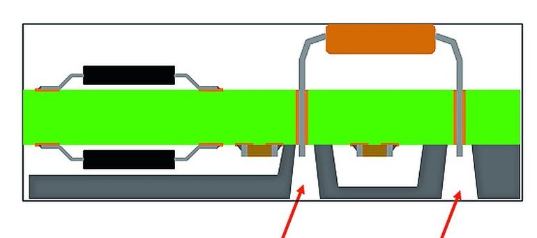
Typically, wave soldering will require a pallet to protect the SMT components that have been mounted in the previous steps. Often these pallets are quite thick, making it difficult for the wave solder to flow effectively and create an acceptable through-hole solder joint. The Pin-in-Paste (PiP) process can often be used to replace wave soldering and have completely eliminated this method. Here we provide an overview of a practical approach to implementing PiP.
First pass yields as low as 10 % are not uncommon in such sophisticated manufacturing processes as described above. The resulting rework required is not only expensive, but can cause serious reliability problems if not correctly performed. Some assembly processes build products with relatively low profit margins. In these manufacturing procedures, the operation and maintenance costs of wave soldering can also make the manufacturing of a product cost prohibitive.
The objective
The objective of PiP is to enable the SMT reflow process to produce acceptable through-hole solder joints, which comply with IPC standards. The aim is to achieve a joint that has no voids and features a solder fillet.
The process
The typical PiP process is incorporated directly into the SMT manufacturing procedure. This approach requires the following:
- The stencil must be designed such that the correct amount of solder paste can be printed onto the through-holes to form an acceptable joint after reflow.
- The solder paste should be amenable to the PiP process.
- The stencil printing process should be optimized.
- The through-hole components selected must be able to withstand reflow soldering temperatures.
- The through-hole component leads must be rounded at the end.
- The through-hole component leads must be of the correct length to form a good solder joint.
- The through-hole components must be mounted correctly.
- The reflow profile will be acceptable.
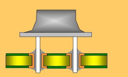
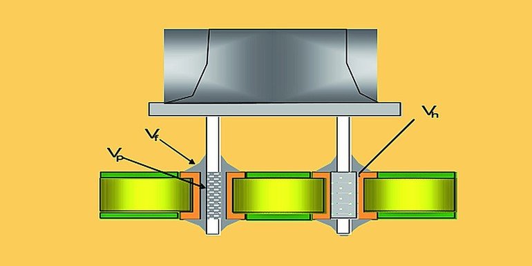
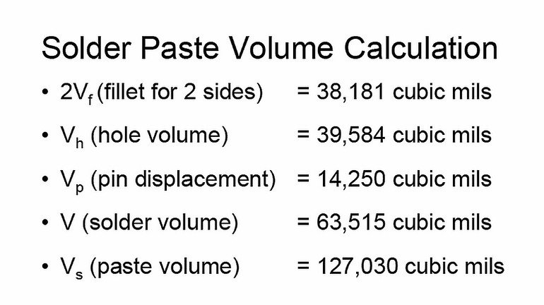
- The greatest challenge in the PiP process is stencil design. The stencil must deliver the correct amount of solder paste to the through-hole in the printing process. To achieve this goal, the amount of solder needed must be determined. The figure which shows the geometry of an acceptable solder joint helps to understand how to calculate the solder volume for through-hole parts.
Stencil design
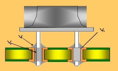
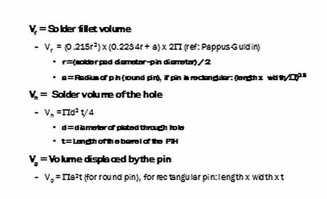
The volume of solder in the through-hole solder joint is defined by these relations: VSJ equals the volume of the through-hole, Vh, plus the volume of the fillet, Vf,minus the volume of the pin, Vp. The equations for these three sub-volumes are given in the figure describing their relations. The volume of the fillet is determined by the Pappus-Guldin theorem for volumes of revolution. Hence, the solder joint volume is:
VSJ = Vh + Vf – Vp Equation 1
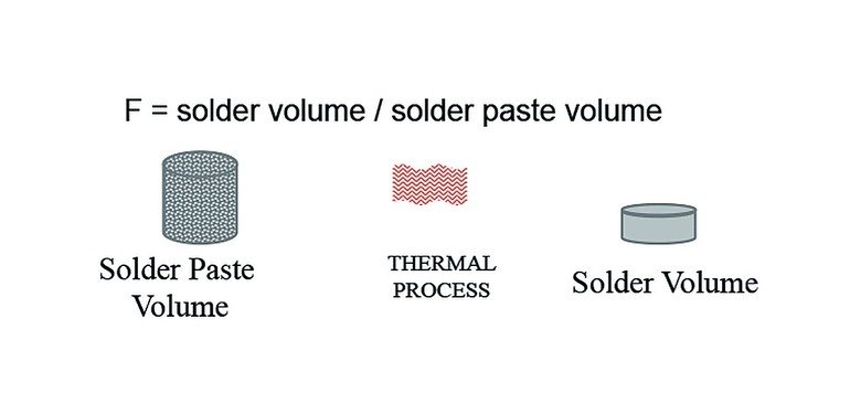
The amount of solder paste that needs to be printed, VSP, is not VSJ, since solder paste is only about 50 % by volume solder. Therefore, the solder paste needed is:
VSP = VSJ / F Equation 2
Where F is the solder paste reduction factor, typically between 0.45 to 0.55. The figure showing the influence of the thermal process demonstrates the solder paste reduction factor in principle.
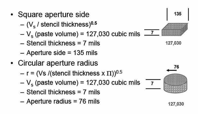
The stencil aperture must be designed so that it provides the needed solder paste volume. If the aperture is circular, the solder paste volume will be:
VSP = r2 t Equation 3
Where r is the aperture radius and t is the stencil thickness, the aperture radius and stencil thickness must be such that equation 3 is satisfied.
If the aperture is rectangular, the equation for solder paste volume becomes:
VSP = l w t Equation 4
Where l is the aperture length and w is its width.
Stencil design example
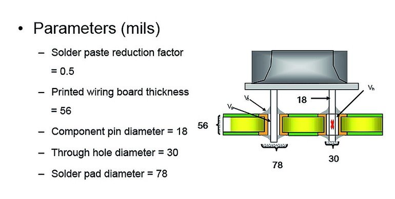
As an example, consider a through-hole component and printed wiring board (PWB) combination as shown in the figure.
Using the metrics from the solder paste volume figure, the equations for the geometry of a through-hole solder joint in the respective figure, as well as the equations 1 and 2, we are able to calculate the solder paste volumes.
Assuming, for example, a 7 mil-thick stencil, the side of a square aperture would have to be 135 mils to provide the needed solder paste. If the apertures were circular, a 76 mil radius would be required. The calculation results for square and circular apertures can be seen in the figure covering the different values.
In PCA designs using fine-pitch through-hole components, rectangular apertures will be required to obtain the desired solder paste volume for those through-holes. In some cases, one stencil thickness cannot satisfy the needs for PiP and other components. In these situations, it may be necessary to print twice with two separate stencils or use a step stencil1).
Stencil design software
Calculating the necessary stencil designs for a particular PCA can be cumbersome. In light of this situation, StencilCoach2) software has been developed. This software enables the rapid calculations of all of the PiP stencil parameters.
Solder paste
The proper selection of a solder paste is crucial in a successful PiP process. Because solder paste is only printed on one side of the substrate, the PiP process relies on the ability of the paste to wet through the board opening to the end of the component’s pins. The solder paste activity necessary to achieve this wetting is process and product dependent. Although there are some exceptions, industry standard Type 3 solder powder is acceptable for PiP applications.
Both no-clean and water soluble solder pastes can be used successfully in a PiP process. However, a no-clean is probably the preferred paste for cleanability reasons. When using solder paste to assemble a through-hole component, there is significantly more flux residue left over than with wave soldering. This thick layer of flux residue will be more difficult to clean than the residue around typical surface mount components. In addition, the component itself can shield the flux residue from much of the cleaning water pressure and rendering it a less effective cleaning process on through-hole components.
Stencil printing
In PiP, the stencil printing process becomes a delicate balance between the requirements for traditional surface mount devices and through-hole components. The printer set-up is key to depositing a sufficient volume of solder paste on the through-hole pads without printing an excess on fine-pitch surface mount pads. Although the exact printer parameters necessary will be process dependent, the most important variables include pressure and print speed.
Pressure: As the squeegee blade pressure is increased, more solder paste is forced into the hole through which the component pin will be inserted. The more solder paste that is deposited, the more robust the through-hole joint will be. If the pressure is increased too much, bridging will be seen on fine-pitch surface mount pads. In addition, a higher pressure will require an increased under-stencil wipe frequency.
Print Speed: The squeegee print speed should be adjusted in conjunction with the squeegee pressure. In general, a slower print speed will allow for a more complete aperture fill and, therefore, result in a greater volume of solder paste deposited.
The emergence of enclosed print head technology (e.g. DEK Proflow, MPM Rheometric Pump, etc.) gives the assembler an added opportunity to further improve the PiP process. Although a detailed description of how this technology works is beyond the scope of this article, information shows that the direct downward force utilized by these systems forces more paste into the hole than the standard squeegee blade printing process. The increase in the amount of solder paste deposited helps achieve a more complete fillet and a more robust solder joint.
Component concerns
Obviously, the components need to be able to withstand the temperature of the reflow process. This information should be available from the component vendor specification sheets.
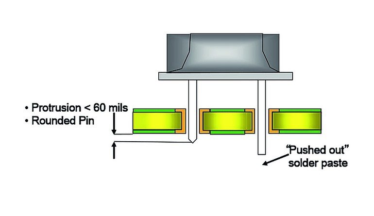
The calculation for the solder paste required to form the desired solder joints does not allow for the component pin pushing the solder paste completely out of the through-hole. To avoid this problem, the component leads should not protrude more than 60 mils from the bottom of the PWB. The leads should also be rounded. The rounding of the leads minimizes solder “push through.”.
Placement
Most assemblers have found that hand mounting works best for PiP. Operators need to assure that none of the previously mounted SMT components are disturbed, and that the through-hole components are mounted such that the pins do not protrude more than 60 mils from the bottom of the PWB. Care must also be taken if the through-hole components have mounting supports that snap into the board. When mounting such components, the snapping action may shake the board and dislodge SMT components.
Reflow
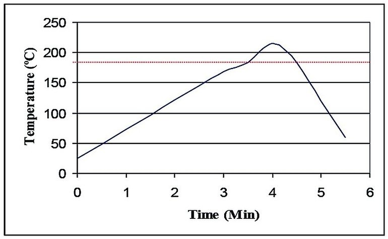
Although one’s first thought would be to use the reflow profile recommended by the solder paste manufacturer, first trying the profile proposed by Lee3) may produce higher yields. This profile has a gentle ramp up at 0.5–1.0 oC/s, a slight dwell at the liquidus temperature, a minimum time above liquidus and a rapid ramp down, but less than 4.0 oC/s.
This profile has been shown to minimize many soldering defects such as solder balling. For the PiP process, the gentle ramp minimizes any viscosity drop in the solder paste due to heat input. The higher viscosity reduces the chance for the solder paste to “drip” off the component during the initial heating stages of the oven. For a detailed discussion of the benefits of this profile4).
Process optimization
The preceding discussion should give the reader reasonable starting points for the PiP process. However, it should always be understood that designed experiments (DOE) are usually required to optimize any process. Once the process is optimized, statistical process control (SPC) techniques should be used for process control. Cost-effective training on DOE and SPC techniques is available.
Conclusion
The PiP process is often the answer to the difficulties of wave soldering complex PCAs. By following the suggestions in this paper we believe that most assemblers can implement a successful PiP process.
Share:


