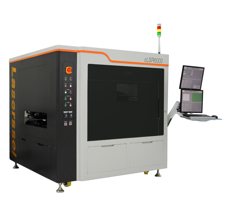
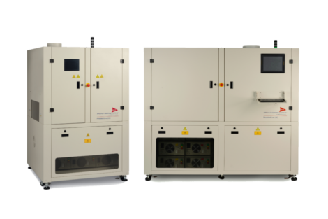
Korean provider of laser selective soldering technology, Laserssel has unveiled the CLSR 6000 Laser Compression Bonder for semiconductor packages. This soldering technique uses high accuracy compression tools and Area Laser bonding introduced with LSR (Laser Selective Reflow) in order to minimize warpage on extremely thin packages and substrates, the company said. This technology has been adopted for high-end 2.5D packaging with dimensions larger than 60×60 mm and NAND modules thinner than 50 µm.
LCB is able to produce thin and large semiconductor packages with very high production yields at low cost that are now considered to dominate technology trends of top tier semiconductor and packaging providers.
The BSOM (Beam Shaping Optical Module) technology takes the energy of a spot laser and turns it into a uniformly distributed area laser. The uniformity of the energy is greater than 95 percent. This means that the energy of the spot laser is spread out evenly allowing for the same amount of energy density over the entire area to be soldered. This enables the proper coalescence, wetting, intermetallic formation to take place, forming the final electronic interconnect or solder joint. Laserssel designs and manufactures this technology in-house.
