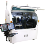
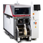
At Productronica 2021, ASM presented in its advanced packaging area solutions for the latest SiP generation, including its new die-bonder, the AMICRA NANO, and its SIPLACE TX micron.
Precision die-bonder
With an accuracy of 0.3 microns @ 3 sigma, the company says its AMICRA NANO can be considered the most precise die-bonder in its class. “Due to its outstanding placement accuracy and support for a eutectic high-speed bonding process, the die and flip-chip bonder is particularly well suited for the reliable handling of ultra-small and very thin chips,” the company said. “ASM AMICRA has developed high-resolution imaging systems to support the dynamic alignment system, implemented a fiber laser as the primary heat source for eutectic die bonding, and installed high-resolution motion control systems on a granite base with a special vibration damping system. At the heart of the [the] image processing-controlled die-bonder, four imaging systems are mounted in fixed positions on a granite base while all other motion control systems move around the imaging cameras. This design concept has been an essential factor in the development of high-precision placement systems to this day.”
High speed for high density
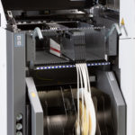
“With up to 96,000 components per hour, placement accuracies of 25, 20 or 15 microns @ 3 sigma and minimum placement distances of as little as 50 microns, the SIPLACE TX micron stands for advanced packaging and high-density applications with unsurpassed productivity,” the company said. “The highest accuracy class is achieved with a new vacuum tool that features an exchangeable magnetic plate for rapid product changeovers. The new 4-mm versions of the Smart Feeder Xi also play a role in the fast and exceptionally precise pickups of even the smallest components and dies. They use the latest micro-tapes and vacuum-level the bottoms of the blister pockets to prevent inclined positions of components within the tape.”
Thin-die
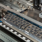
“Since thin dies, flip-chips and the smallest 0201m components require extremely gentle handling, the whole placement process of the micron can be individually programmed for each component and placement position with features like touchless pickup and zero-force placement. And for sensitive thin dies, the vision system features advanced image processing algorithms such as cracked-die inspection and die-chipping detection. This way, components with hairline fractures and lacerated edges are detected and rejected already during the pickup process.”
A space saver
The company says the new micron occupies a footprint of only 2.23 by 1.0 meters (approx. 7.3 by 3.3 feet), which makes it a particularly attractive option for tight cleanroom environments thanks to its DIN EN ISO 14644–1 Class 7 certification.
Integrated smart factory
The micron features a broad range of M2M and networking capabilities. Open and standardized interfaces such as ASM OIB, IPC-HERMES-9852, IPC-CFX and IPC-SMEMA-9851 allow it to be fully integrated into workflows, higher-level MES/ERP systems, traceability solutions, and the integrated smart factory, the company confirmed.
