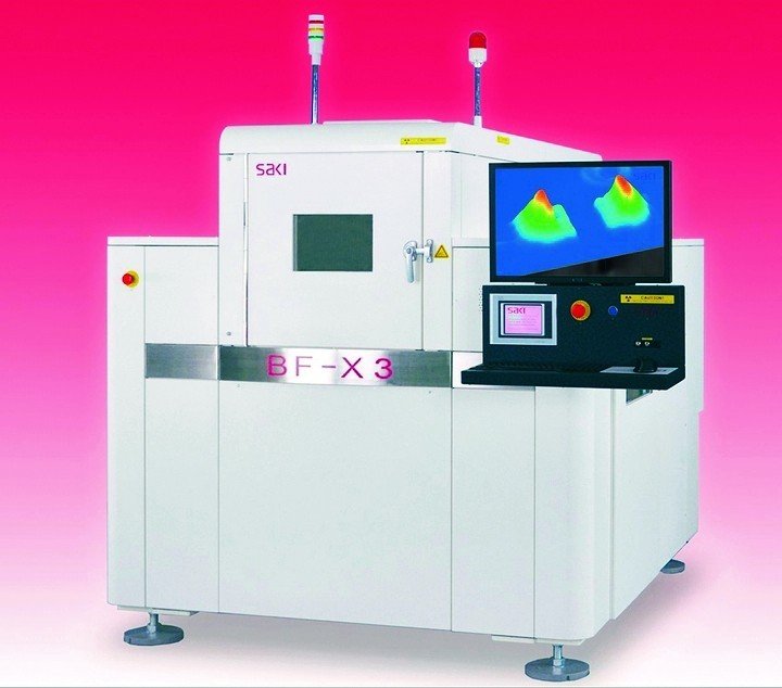
Saki Corporation showed the BF-X3 in-line 3D automated X-ray inspection system measures solder joint structures, even non-wetting and head-in-pillow, creating 3D data for every solder joint. It uses planar computed tomography (PCT) to capture 100 slices through the board, solder joints, and components, analyzing their internal structures for a true volumetric representation of 3D imaging. Automated inspection technology perfectly separates the top and bottom of the PCB, corrects position misalignment and warpage, and measures and classifies defects, creating 3D data for the entire sample. It gives best-in-class Cpk and gage repeatability and reproducibility and maximum test coverage with lowest escape and false call rates. The BF-X3 inspects and measures the solder joint structures of BGAs, LGAs, QFNs, plated through-holes, leaded ICs, and PoP lamination in 3D with high definition.
The BF-3Di uses its unique optical design and 4-way projection for 3D inspection of all parts on the PCB with brightness controlled and shadows eliminated. It inspects heights up to 20 mm and parts as small as 01005s, capturing reversed or inclined components with an escape of less than 1 ppm. Its high-speed, real-time measurement for a broad range of substrate coverage greatly reduces programming and debugging time. Inspection data is quickly and easily generated from CAD data.
For offline 2D automated optical inspection, especially for double-sided boards, the company showed its BF-10BT system. It inspects both sides of the board in one process, detecting solder balls down to 150μm, with 10μm resolution and superior data handling. Its robust and highly repeatable hardware is built for 24/7 continuous operation. The system is perfect for final inspection, through-hole inspection after wave or selective soldering, and manual inspection.
Share:
