Bottom terminated components (BTCs) are one of the most important components in electronics today. Their combination of small size, excellent electrical performance, and ability to transfer heat away from the integrated circuit (IC) has resulted in their becoming one of the most common packages with the highest growth rate. More than 15% of all electronic packages assembled are BTCs, with their numbers over 50 billion a year. One of the most common BTCs is the quad-flat pack no-leads (QFN). One of the primary attributes of QFNs is dissipating heat, therefore, any voiding of the solder connecting the thermal pad on the QFN to the printed wiring board (PWB) will degrade the intended performance of the QFN. This degraded thermal performance may result in reliability and operational issues. While degraded thermal performance may not be a critical issue for some consumer products, the rapid growth of automobile electronics and the emergence of 5G telecom equipment makes robust thermal performance of QFNs vital.
Original investigation
Generally, there are no industry standards as to what is an acceptable voiding level, although there is agreement that an average void area should be less than 50% with no single void above 40%. For thermal pads, a void area of less than 25% is preferred, and some automotive applications aim for an average void area of less than 10%. Clearly, all assemblers desire a minimum amount of voiding. However, the processes and materials available may limit this goal.
Significantly reducing voiding is not necessarily a quick fix. Optimized solder paste and process conditions; control of the PWB and components; and a stencil printer, component placement equipment, and a reflow oven that are optimized to minimize voiding are needed.
In our experiments, the PWB pad finish was ENTEK Plus CU-106A-HT OSP. We used laser cut, non-nano-coated steel stencils that were 0.004“ and 0.005“ thick. We used a window pane stencil design in the PWB thermal pad area to allow volatiles to escape. The window pane squares were 0.088“ on each side. The squeegee printing speed was 100mm/s with a pressure of 6 kg. Printer separation speed was 5mm/s at a distance of 2mm. We performed a stencil wipe (W/D/V) before each board. The QFN we assembled had a square ground plane of 7.75mm (0.30“) per side.
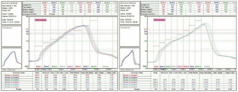
We performed reflow in air with Profile #1—a straight ramp profile (0.9˚C/second ±0.1˚C/second) and a peak temperature of 241˚C ±4˚C for most investigations. However, a second profile (Profile #2) with a peak temperature of 254˚C ±4˚C was also investigated to determine the effect of the reflow profile on voiding. A variety of solder pastes was used that had halogen-free and halogen-containing fluxes and different solder particles sizes (e.g., Type 3, Type 4, Type 4.5, and Type 5).
Reflow profile effects
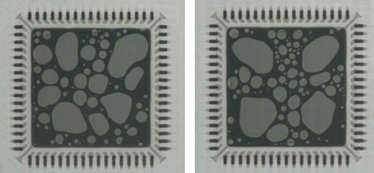
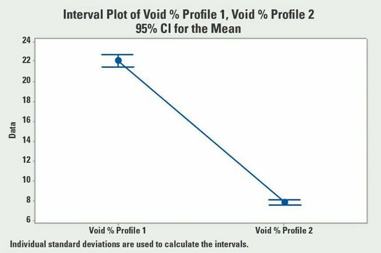
Profile #1 is a ramp-to-peak profile with a maximum temperature of approximately 240˚C ±4˚C. Profile #2 has a slight soak and a peak at 254˚C ±4˚C and has a slightly higher time above liquidus of 77 seconds versus 70 seconds.Profile #2 had significantly better voiding results, yielding less than 8% void area versus 22% for Profile #1. Not only does Profile #2 significantly reduce the area of voiding, the scatter in the data is also greatly reduced.
Our theory is that the hotter profile is more successful in driving out the volatiles than the cooler profiles. This concept is easy to understand when one considers that the vapour pressure of most solvents increases considerably at higher temperatures.
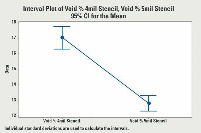
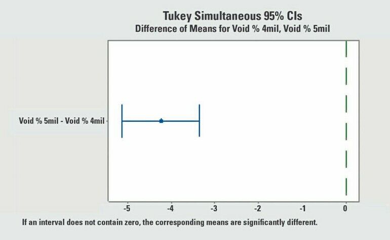
Stencil thickness
We performed experiments in the conditions described with Profile #1 using two stencil thicknesses of 4mils and 5mils. A Tukey analysis indicated that this difference is significant. We believe that the 5mil stencils exhibit less void area because the higher stand-off (0.005“ vs. 0.004“) allows for easier outgassing/venting of the solder paste flux volatiles.
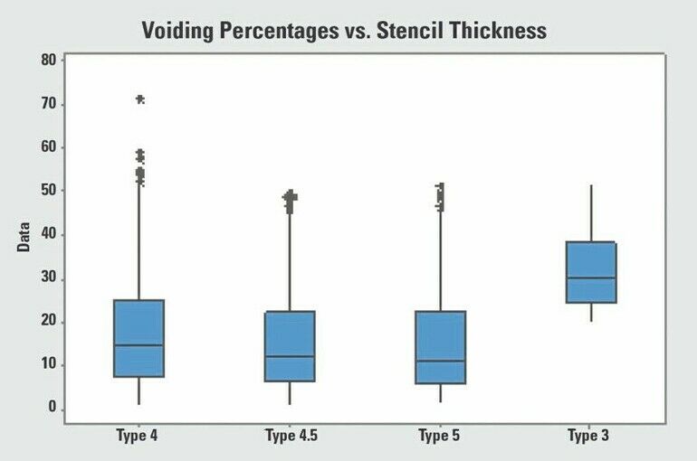
Solder paste particle size
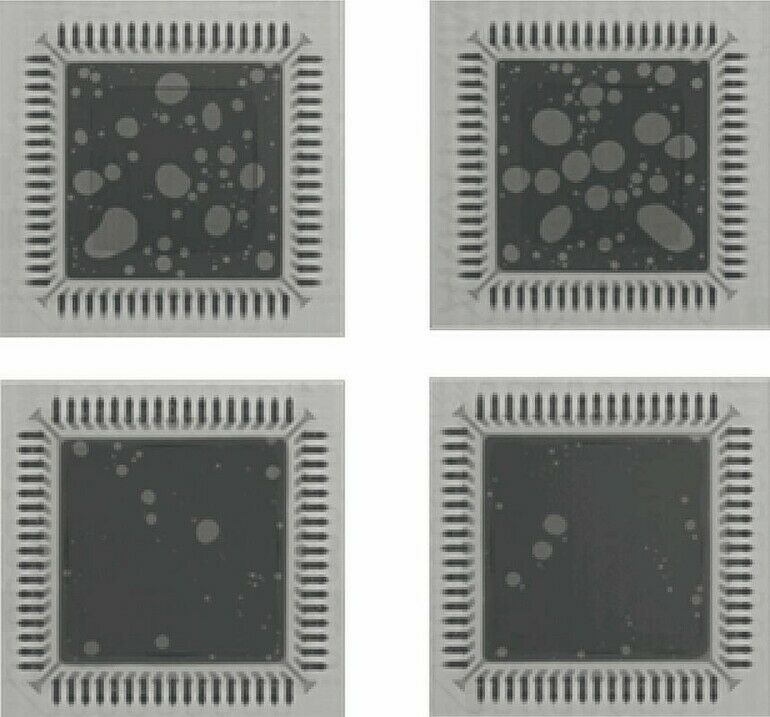
We experimented with varying the solder paste particle size. The stencil thickness of 0.004“ and Profile #1 were used. The results of this indicate that there appears to be a slight reduction in void area with small solder paste particle sizes going from Type 4 to 4.5 to 5; however, there is a significant increase in voiding area percent with Type 3 paste.
Solder pastes
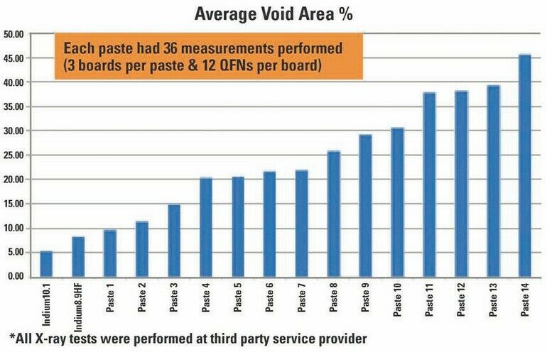
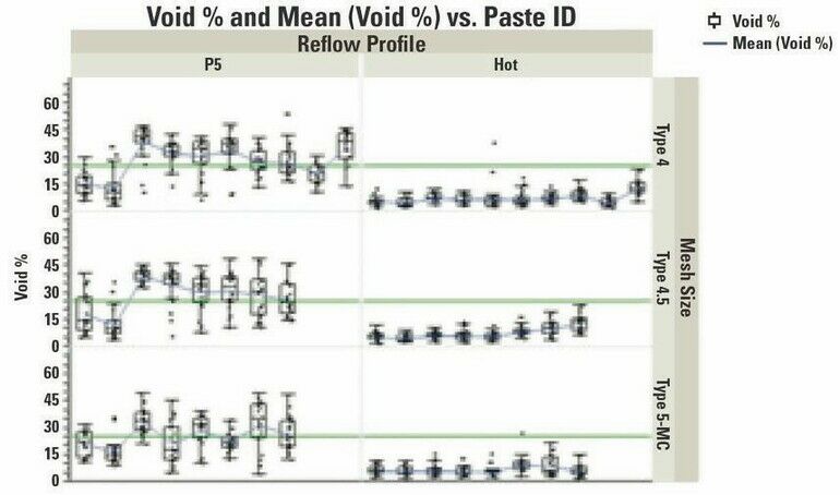
We performed a final experiment in which we evaluated the effect of different solder paste flux vehicles on voiding. Three PCBs with 12 QFNs each were used for each solder paste, for a total of 36 QFNs per paste. The results were striking, as seen in Figure 11. Some pastes produced about 5% voids, while others produced as much as 45%. These results were not only surprising, but also very encouraging.
While the generation of voids is a complicated process with many variables, selecting the solder paste alone, with a standard assembly process can assure voiding area levels of less than 10%.
Conclusions
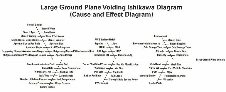
Although the factors that generate voids are many, by adopting a standard process as described, several parameters can be set to minimize voiding. The strongest determinant in the assembly process is to have a hotter peak temperature reflow profile. This factor alone reduced voiding area percent from an average of about 22% to less than 8%. Although finer solder particle size reduces solder voiding, the result was only statistically significant by going from Type 3 to Type 4 or finer. Type 3 pastes produced more than 10% more void area than Type 4 or finer.
Using a stencil thickness of 5mils reduced voiding about 4% on average as compared to 4mil stencils. The greatest surprise, however, was how significant solder paste formulations were in reducing voiding. The better solder pastes significantly reduced voiding to less than 6% void area, whereas the worst paste produced greater than 45% voiding.
Productronica, Booth A4.309
To be continued…
The second part of this paper, in which Flanagan, Belfield, and
Hotvedt detail the additional
investigations they have undertaken to identify and refine void reduction strategies will be published in our April 2024 issue.


