While harsh environment testing requirements have continued to increase, there have also been broader trends of advancing electronics density, voltage, and miniaturization. Ensuring end product reliability necessitates taking all of these changes into account throughout processing. As a solder manufacturer, Indium Corporation has seen how the automotive electronics’ trend toward harsher test conditions has required a few relatively major changes to the solder paste material itself.
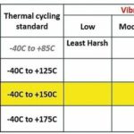
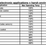
The conditions outlined by the International Electronics Manufacturing Initiative (iNEMI) as “Elevated harsh” or the even greater “Severe harsh” have caused a shift away from standard SAC alloys towards those that are generally considered “high-reliability alloys” for specific applications. Thermal cycling tests from -40 to +150 °C replicate extreme operating conditions and ensure good performance therein. Despite efforts to make high-reliability alloys “drop-in” solutions, it is important to remember that these alloys are metallurgically complex. They enable enhanced thermal cycling performance, although the alloy is not the only variable in the equation. Thermal cycling can also be impacted by other factors, including the flux vehicle, component type, surface finish, and processing conditions among others.
Miniaturization of high impact
A fact that can occasionally be lost in the excitement of drastic innovation is that there are changes that do not necessarily increase performance requirements, but steadily increase the challenges of reaching existing quality and reliability standards. Miniaturization is a trend that revitalizes “old” necessities related to printing and processing. The impact of miniaturization is relevant across many applications due to a shared increase in expectations for electronics. The expanded everyday use of electronics and its integration into lives, homes, and vehicles operation and, in turn, are driven by miniaturization. Familiar metrics can continue to be used– such as area ratio, print transfer efficiency, and standard deviation– for these soldering processes, as long as their new context in relation to miniaturization is understood.
As components shrink, so do their respective stencil aperture sizes. Reduced aperture areas give rise to more challenging solder printing conditions. Traditionally, the recommended area ratio (area of the stencil opening / area of the stencil walls) is greater than 0.66; however, as component sizes have decreased, that recommendation has become relaxed.
The current smallest commercial chip (the Murata Manufacturing Co., Ltd. 008004) is 0.25 mm in length and 0.125 mm in width. The 008004 is cutting-edge technology and its diminutive size is arguably not an immediate concern to most manufacturers, however, even the larger 0.4 mm by 0.2 mm 01005 chip requires pushing past previously definitive boundaries in electronics manufacturing. 01005 chips may have aperture area ratios of approximately 0.5.
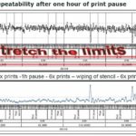
Once the end of the 0.66 limit to aperture area ratios is acknowledged, it is inevitable that materials and processes will be stretched in the search for the next limit. These limits will continue to be pushed by varying both the soldering material and the process conditions. There are two primary constituents to vary and optimize in solder paste:
- Powder size and distribution
- Flux chemistry
On the other hand, there are numerous variations to PCBA process conditions, including, but not limited to:
- Print speed
- Gasketing and clamping
- Squeegee pressure
- Stencil coatings
- Aperture shapes
- Temperature and humidity
Powder size and process capability
The selection of solder powder size distribution is a well-defined method for improving print performance at reduced aperture ratios. A Type 4 particle distribution ranges from 20-38 µm in diameter and for the average application, it is the first paste to be considered. Every variety following Type 4 is generally an acknowledgment of some challenging stencil design, aperture area ratio, or built-in processing restrictions.
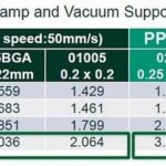
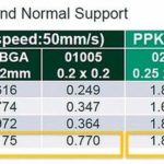
A print study was conducted, depicting the values of Cpk (Process capability index). As expected with decreasing component size and the associated minimized stencil aperture size, the printing performance decreased. However, the study also showed that miniaturization increased the relevance of every other parameter. When printing a deposit for a 0201 component, all four powder types and all four printing conditions demonstrated well-controlled processes with Cpk values over 1.66. There is a flexibility for the 0201 components because the area ratio is typically at least 0.66.
Indium’s automotive-grade solder paste for enhanced electrical reliability
However, the study also demonstrated that although it may be necessary at times, changing powder type is not a simple fix in regard to miniaturization. Without vacuum fixturing support and with top clamping, even Type 5MC solder paste did not enable consistent and controlled printing for 01005 components.
The other major component of solder paste–flux–is somewhat less neatly categorized. Yet, the thixotropic rheology of flux is still an important attribute to the solder paste printing performance. Flux composition is made up of four major categories of materials that control the chemical activity and physical characteristics of the solder paste:
- Resins serve both as an oxygen barrier and also as a tacky and viscous component in flux.
- Gelling agents control the viscosity, stability, and related rheological properties of a paste.
- Activators dissolve oxides and promote wetting as an active chemical cleaner during reflow.
- Solvents dissolve the resins, gelling agents, and activators to ensure a homogeneous flux vehicle for solder paste.
The challenge regarding solder flux selection is the potential to affect many other processing steps beyond print transfer efficiency. The different constituents within flux chemistry may be optimized for other characteristics, such as low- or high-temperature reflow, low voiding, stability, and surface insulation resistance (SIR) performance. Modern no-clean fluxes have improved to the point where they can generally be optimized for a specific performance metric and also retain good rheology for print performance. However, it is worth remembering that as aperture sizes shrink, previously negligible differences become more noticeable and significant.
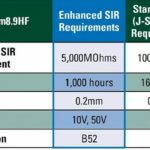
Flux characteristics other than print performance can also be impacted by the changes in electronics’ density. In particular, SIR performance challenges are complicated as low-standoff components become more common. The components may not be as noticeably impacted by the printing process, but they carry an increased risk of corrosion due to retained flux solvent at the narrowed underside. Enhanced SIR expectations beyond J-STD-004B have already become relevant due to a separate trend of increasing voltage in automotive power-train electronics. Both changes–the trapped solvent and increased voltage–increase the risk of electrochemical migration and dendritic growth.
Novel enhanced SIR tests reflect new expectations. Reduced line spacing and increased voltage during testing are some of the significant changes that are verifying long-term reliability in the face of increased electronics density and voltage potential within actual products.
Outlook
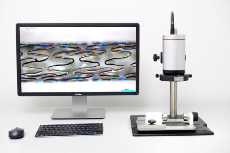
Indium Corporation believes that material science changes the world. When the current trends in electronics manufacturing and PCB assembly create and enhance process challenges, their focus is always on developing new solutions for current and evolving needs. Nevertheless, the existence of these trends has been enabled by the industry’s increasing capability to identify and address these challenges. New standards and tests are used to develop and verify solder material reliability. Other improvements, such as those to stencil technology and fixturing, have become more common now that new applications demand them. Solder paste inspection (SPI) systems are now more powerful than ever, capturing valuable data on shrinking deposit sizes and provide real-time print process statistics. The tools and technology are available as long as the users are diligent in their application.
Andreas Karch, Regional Technical Manager for Germany, Austria, and Switzerland and Claire Hotvedt, Product Development Specialist for the PCB Assembly business unit, Indium Corporation
Die Anforderungen in der Automobilelektronik steigen ständig und der Auswahl der Lotmaterialien kommt höchste Bedeutung zu. So dürfen Lotpaste, Flussmittel sowie Fertigungsprozess die Zuverlässigkeit der Automobil-Baugruppen, in denen auch höhere Spannungs- und Strompegel verarbeitet werden, keinesfalls beeinträchtigen.
Alors que les composants électroniques pour les automobiles sont soumis à des exigences de plus en plus strictes, la sélection des matériaux à braser revêt une importance majeure. Ainsi, la crème à braser, les flux et le processus de production ne doivent en aucun cas nuire à la fiabilité des équipements automobiles également soumis à des tensions et des intensités élevées.
Требования, предъявляемые к автомобильной электронике, постоянно растут, и выбор материалов для пайки имеет первостепенное значение. Паяльная паста, флюс и процесс производства не должны снижать надежность автомобильных узлов, в которых могут присутствовать более высокие уровни напряжения и тока.
Indium Corporation
34 Robinson Road
Clinton, NY 13323 USA
Tel.: +1 (315) 853-4900
Website: www.indium.com
