
When considering a PCB-A with THT power electronics, quality assurance criteria can be divided into 3 areas: components on the top side; pins with solder joints on the bottom side; and the barrel fill through the PCB. The fulfilment of these criteria requires specifically configured inspection systems which have been adapted to the respective production step and the type of defects.
Combining assembly and inspection
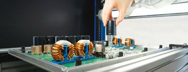
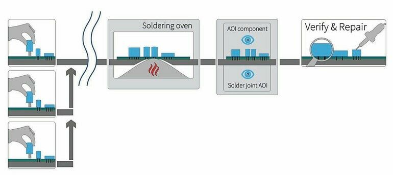
Typically, the manufacturing of THT power electronics begins at assembly workstations where the THT components are manually mounted on the PCB. An automatic inspection at this stage in the process offers the greatest efficiency through a short quality control loop. Failures like a wrong polarised electrolytic capacitor can be detected and corrected immediately without the use of a soldering iron. Camera modules mounted directly above the assembly workstation can be used to carry out this task – and can conduct the inspection almost without the operator noticing. Another advantage of a quality check at this production stage is that, even if down holders are used for the PCB-A, the components at the workstation remain in direct view whereas, in subsequent stages, test objects may be covered. Typical component inspection at this production stage involves testing for: presence, polarity, labelling (OCR) and colour, as well as reading the serial number of the individual PCB.
3D for high solder quality
After the defect-free mounted PCB has left the combined assembly and inspection workstation, it can be fed into the soldering process. To detect defects at this stage, AOI systems are typically used to inspect the THT solder joints on the bottom side of the soldered PCB. The AOI system must, in this case, fulfil two main requirements. Firstly, it must inspect the PCB-A from below, as turning would mean an enormous additional effort. Secondly, in order to measure solder volume and pin length, a 3D system is required.
AOI system in the THT process
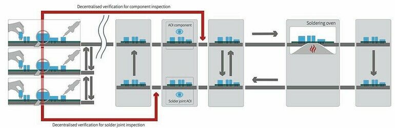
Depending on the process sequence, product variety and planned budget, component inspection can also be integrated directly into the production line. This can be done, for example, by integrating a double-sided AOI system after the soldering oven. Possible disadvantages of this, however, are higher costs for repairing the component defects as well as the potential covering of parts of the PCB-A by down holders.
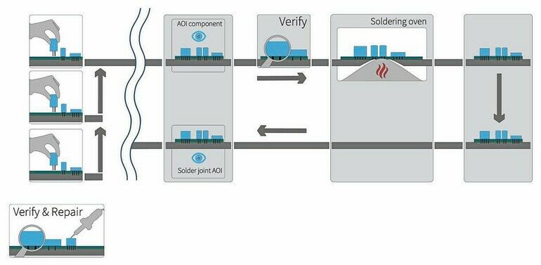
The use of AOI systems in the THT process is highly efficient in production lines that provide return transport of the carriers (including PCBs). In addition to an optimised product transport sequence, this setup offers additional possibilities for the integration of optical inspection technology. For example, two AOI modules can be integrated into one housing in front of the soldering oven to save space. Components with defects can be redirected and repaired ’cold’ before soldering. In this case, solder joint inspection will take place in the same basic system but with a time delay in the lower return transport of the PCB-A.
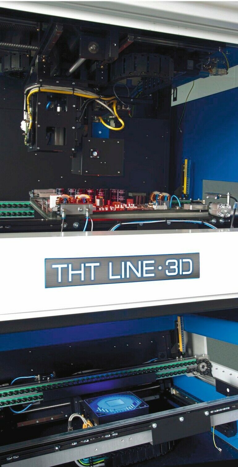
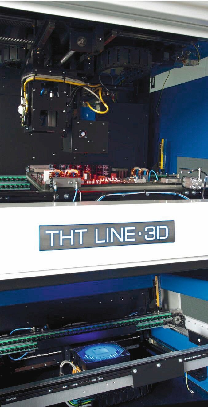
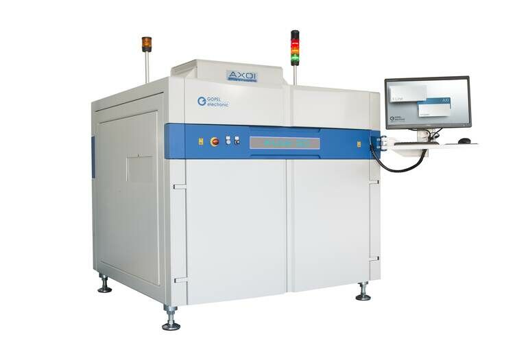
Integrations like these are possible using the THT Line 3D AOI system, which offers configuration options for different AOI modules in both the upper and lower transport module, meaning different inspection programmes can be executed simultaneously. Depending on requirements, orthogonal inspection modules with or without angle view cameras as well as 3D measurement modules are also available.
The integration of verification and repair stations contributes to the efficiency of the overall process in a way that should not be underestimated. In conventional line concepts, these are often located directly behind the respective inspection system. Even though, in such cases, the evaluation and further processing of the PCB-A takes place immediately after the AOI inspection without any loss of time, this approach has some disadvantages. Verification at this central point requires either an additional dedicated person or ’jumpers’ from the respective assembly stations – both of which lead to increased use of resources.
Reducing resources
A solution for reducing this type of expenditure is a decentralised verification of the faults detected by the AOI systems from the respective manufacturing stages for all lines. This is possible if the faults from the inspected PCB-A are instead presented at the workstation. The PCB-A remains in the AOI system or on a conveyor module until the complete classification of all faults has been carried out “remotely”. This decentralised classification has a learning effect that is very valuable for continued quality improvement as operators are faced with their “own” failures. The PILOT Connect communication system offers convenient verification via an ethernet connection to the appropriate position in the production line. Depending on the existing line control system, a faulty PCB-A can then be transported directly to the respective workstation for rework.
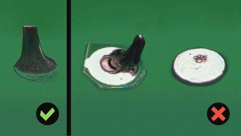
These types of faults are visible on components, pins or the PCB-A. However, the third ’quality check’ is also critical as it evaluates the solder filling from the bottom to the top of the PCB. In the automotive sector or in other safety-reliant applications, this is often a particularly important quality measurement.
High quality based on perfect interaction
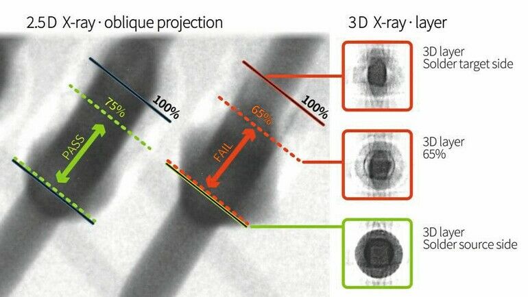
Regardless of whether utilising 2D nor 3D technologies, AOI inspection cannot be used to reliably measure solder filling. The only way of doing this is with X-ray technology. But even this method requires a performance analysis to determine whether a particular measurement can be carried out using the technology at hand. A solely 2D X-ray system is not able to determine the filling of the solder so precisely that it can reliably confirm if specific requirements (e.g. min. 75%) have been fulfilled, for instance. X-ray systems with tilt view offer the possibility of getting a view of the filling level of the solder joint; however, this can prove difficult in practice, especially for connectors with a high number of pins since closed pin overlaps are to be expected. This can, in addition, lead to increased effort when it comes to test program generation as the imaging method causes perspective distortion and thus CAD data for the PCB-As cannot be used for automated program creation. Optimal results for measuring solder filling can be achieved using a 3D-AXI system. Due to the standardised view of the solder joints in the X-ray image, pre-defined inspection functions can be used – greatly reducing the programming effort. The evaluation of the solder filling in individual layers also guarantees an exact measurement of the fill level as well as the detection of voids.
In conclusion, achieving secure and efficient quality assurance for THT power electronics places complex demands on inspection systems in terms of both technology and flexibility. The integration of verification and repair stations also plays an important role. Suppliers of handling and inspection technology should be involved at an early stage in process planning to help jointly develop an optimal line concept.
SMTconnect, Stand 4A.227


