When the paths of two industries cross, the market will drastically change, new rules will apply and established settings no longer exist. This happens right now in the semiconductor and SMT industry for SIP and other related packages.
Hitachi High-Technologies Europe, Krefeld (Germany)
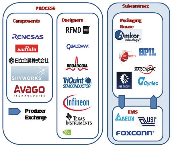
With the higher integration of smart phones and tablets a wide base of mainly American designers enjoy a hectic life on a fast track, under extreme time pressure, facing high technical barriers and cost pressure. Many of these design houses have no real fab capability and rely on outsourcing.
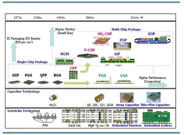
Miniaturization goes on
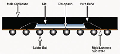
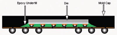
Blue tooth, graphic cards, camera modules, power amp devises, RF modules, flash memories, base band processors, are typical new components in the products with higher integration. Most likely they are designed with two or three flip chips and several small 01005 (0402m) or 0201(0603m) chips. The single devices are bundles in thin laminate strips with sizes around 170mm by 70mm in boards up to 200 per panel pending on the size. The high degree of integration no longer permits the wire bonding technology – so flip chips are the next generation of default packages. The basic drivers of the devices are low cost substrates, high speed bus architecture, broad band RF modules, radar and micro wave. With decent growth rates in 2009 for base band processors in the 20% range the percentage will grow to ABI Research latest forecast. Researchers are forecasting flip chip devices with a 15% to 20% CAGR growth rate. No other device in the industry is increasing at this fast pace. Assuming that the selling trend of currently about 120,000,000 smart phones per quarter continues, the change in the industry will become even more visible than today.
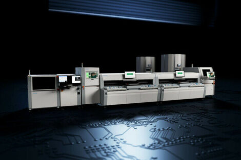
Production floor
Now, looking into the manufacturer sites we see two different worlds. The semiconductor factories with a broad integration of non fab subcontractors in countries such as Taiwan, Malaysia, Korea, China and the Philippines have superb knowledge of placing flip chips, substrate handling, and wafer technology as true semiconductor manufacturers, while their experience placing chips is limited. Also, these companies do not always experience the same cost pressure as typical CEM’s in the SMT assembly market. Also these companies are not always experience the same cost pressure like the typical CEM in the SMT assembly market. On the other hand, not all SMT CEM’s are ready to take on the task of placing flip chips. Beside knowledge, large investments are necessary, including clean rooms. During the last year however, quite a number of blending products are moving in both areas. SMT subcontractors quickly study the flip chip process to be able to get on board. Besides process and material knowledge, there is quite a unique demand for SMT placement machine capability, which makes SIP components processing a challenge. Most suppliers ask for a flip chip placement accuracy of 10μm, 3 Sigma. This reflects future demands while 15μm, 3 Sigma is the requirement for current day to day work. Bump diameters of 80μm with a tolerance of 25% are standard. Other parameters such as, for example, fiducial accuracy drive the accuracy level down to the 15μm,3 Sigma demand. Inspection before and after fluxing are on the must have list. On the chip side, 01005 (0402M) components also require high placement accuracy of under 35μm. Placing the components with a minimum distance of 0.11mm from body to body requires many machine attributes insuring high quality placement and repeatability. Heat dissipation over time, long term accuracy of feeders and positioning system, warpage compensation, XY-print picture compensation are only a few to mention. Wafer handlers feeding directly into the placement machines are the preferred methods for smaller batch sizes while tape feeders are common, particularly for smaller dies. For wafer handlers thin dies are sensitive to handle and require intelligent ejectors. Horizontal feeders have advantages for larger dies. Using wafer mapping and cassette changer are standard practice. Both processes combined require good adaptability for smaller and larger lot sizes. Wafer as well as tape feeding for flip chips need to be possible. The importance to balance ramp up and high volume production is reflected in the financial bottom line. NPI is most likely done with direct wafer feeding while high volume is done with tape feeding. Two floors, one for semiconductor assembly and one for SMT assembly become one production unit. Over the next five years, the future will show who will win this race.
Zusammenfassung
Wenn sich der Weg zweier Branchen im Markt kreuzen, bedeutet das einen dramatischen Wechsel. Neue Regeln werden erstellt und längst Etabliertes existiert nicht mehr. Der Artikel geht hierbei auf die Halbleiter- und SMD-Bestückung ein.
Lorsque deux secteurs d’activité voient leurs chemins se croiser sur le marché, cela représente un changement dramatique. De nouvelles règles sont édictées et ce qui a été établi de longue date n’existe plus. A ce sujet, l’article s’intéresse à ce sujet aux équipements en semi-conducteurs et en SMD.
Share:


