Modern PCBs with a high packing density and a mixture of SMD and THT components are constantly becoming more complex, increasing the demands placed on electronic manufacture. Stencil technology must consequently also go increasingly deeper – the way into the third dimension.
Christian Koenen, Ottobrunn (Germany)
More and more components have different heights for their connections. This is partly due to the tolerances of the manufacturing processes, the physical demands placed on the function, the thermodynamic properties of the components, or due to damage caused during transport or handling of the components. PCBs and substrates face essentially the same problem.
Compensation for coplanarities
It is generally assumed that the soldering paste height has a direct influence on the potential for compensating coplanarities. As a rule of thumb, 50 % of the stencil thickness can be compensated as coplanarity. This general figure is certainly not valid for all designs, however, provides a very general reference value. If we look at the development of the average stencil thickness over the past few years, we can determine a noticeable trend towards smaller thicknesses. Generally speaking, this results in a lower compensation potential for coplanarities. In addition, the requirements placed on the component producers and componentry manufacture also increase as a result of finer screens and a continuously growing variety of components. Components that work in the high-frequency range, for example, sometimes require a geometry adapted to the frequency range. Combined with a high throughput, this may result in differences in height of the connecting surfaces of >1 mm.
Height differences result in contact problems
Depending on the design, height differences in the components pose a problem for surface-mounted componentry already from a height difference of >30 to 50 µm. The problem is due to the soldering process, which requires that the contact surfaces must be cleaned from any soiling and oxides prior to soldering. For this, a sufficiently long contact with the flux is necessary. If, after the assembly, a component connection is not arranged on the surface of the paste depot, the cleaning process can only start once the other connections have sunken into the softening soldering depot or the liquefied soldering metal. Depending on the moment of the contact, this significantly reduces the time for the formation of the solder point. If the soldering period is too short, this may negatively affect the characteristics of the solder point. In the worst case scenario, there is never any contact with the soldering depot on the substrate.
The goal is to develop reliable manufacturing processes that are capable to fulfil the requirements of the components. The modern stencil technology of Christian Koenen can offer technical solutions for these requirements.
Stencil technology in the third dimension
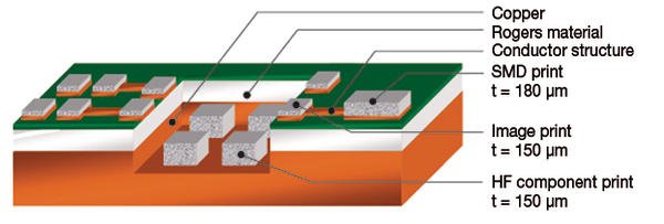
To integrate components in cavities of the PCB (i.e. embed these), it is necessary to go into the third dimension using the la- test stencil technology: the development of the 3D-stencil of the company fulfils these prerequisites. It makes simultaneous printing on several levels of a substrate and the compensation of elevations and cavities on a substrate possible.
At its in-house research laboratory, the Application Center, the company has developed 3D-stencils and squeegee blades adapted to the process, which are capable of following the surface topography. In such complex structures, the requirements and technical processes rely on maximum precision and the latest manufacturing techniques in stencil production. The step technology of Christian Koenen GmbH makes it possible to implement different stencil thicknesses in one stencil. Elevations and cavities can be produced on the squeegee and/or PCB side.
Typical applications for the step technology include:
- Adaptation to the paste requirement of the component
- Change of the stencil thickness
- Compensation for substrate unevennesses / multiple printing
- Cavities in the bottom side of the stencil
- Printing on different levels
- Parallel printing levels in one stencil
These possibilities allow for the development of solutions for handling major coplanarities and connecting surfaces arranged at different heights.
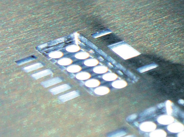
For a number of components, great coplanarity value ranges are already defined in the datasheet. This affects in particular QFPs with ground planes and LEDs with ground planes. These are differences in height between the ground pad and the outer connections, which are combined with the usual coplanarity tolerances. As a result, soldering paste printing requires printing on depots of different heights, so that all connections rest on the soldering depot. For this, the stencil thickness is adapted according to the specifications.
Using the step technology, this is certainly possible as long as the differences in height do not significantly exceed 50 µm. For larger differences, the suitability of the use of the step technology must be tested on a case-to-case basis.
Alternatively, processing without steps is possible: The size of the openings ensure that the ground planes are supplied with the right amount of solder, and the outer connections receive so much solder that any possible distances can be overcome thanks to the convex shape of the soldering surface on the pads. Normally, overprinting of the pads is necessary in this case.
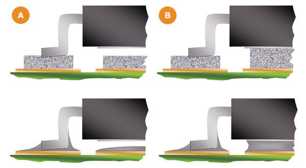
Geometric restrictions
Special requirements for the components functions in some cases result in geometric restrictions on the component design. Especially in the high-frequency range, special designs may be used. Here is an example of a performance component from the HF range: The component has two connecting levels that are arranged up to 1,120 µm apart in the height axis. The electrical connections are at the top, heat dissipation takes place at the bottom. This design places particular demands on the printing technology, as two levels with a significant difference in height must be printed in one printing process here. This requirement is fulfilled by a modification of the step technology, which provides for the creation of two different printing levels in the 3D-stencil. A special squeegee is additionally required, which must be able to print on both levels simultaneously.
Finer screens result in higher demands in terms of the coplanarity of the components. This is due to the reduced stencil thickness with that these screens must be printed to guarantee good release properties. Modern processes in stencil manufacture, like the 3D-stencil technology, offer solutions to these problems. The technology is capable of integrating different layer thicknesses, printing levels and cavities in one stencil, thus improving many critical processes significantly.
ZUSAMMENFASSUNG
Moderne Leiterplatten mit hoher Packungsdichte sowie einem Mix aus SMD- und THT-Bauteilen werden immer komplexer. Die Anforderungen an die Elektronikfertigung steigt. Moderne Verfahren in der Schablonenfertigung, wie die 3D-Technik von Christian Koenen, bieten Lösungen.
Les cartes à circuits imprimés d’aujourd’hui qui présentent une haute densité de composants et une combinaison d’éléments CMS et THT gagnent en complexité. Les exigences posées à la fabrication électronique s’aiguisent. Des procédés modernes de moulage, tels que la technique 3D de Christian Koenen, proposent des solutions à cet égard.
Share:


