Low temperature SMT soldering is not just here but is undergoing ever expanding adoption, being the key enabler to tremendous component & laminate cost savings. Replacing costly wave soldering by a majority of smart adopters enabled shorter process flows that saved not just energy but largely mitigated the damaging effects of thermal shock in wave soldering.
Mitch Holtzer, Alpha Metals, Jersey City, NJ, USA
Take the example of a Molex Shrouded Header. It is $0.84 each for low temperature but the regular variant is $1.23 each at bulk volumes. That is 46% savings right up front for just one connector. Then there is lower temperature molding compound for IC packages. Most other components are cheaper for low temperature. Taking multiples of each component and the types that makes up today’s typical assemblies and it becomes clear why low temperature is the smart way to go.
Components align far better when laminates warp much less due to low temperature soldering instead of Pb-free or SnPb temperatures. Beyond this, low temperature soldering enables finer component pitches and closer spacing as well as increasing component population density over regular assemblies because laminates warp less. Because laminates warp much less at lower temperature, many adopters took the advantage and migrated to less expensive laminate materials for even more savings. Where application permits, already low cost laminates can go even lower as in the following Value-In-Use excerpt.
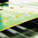
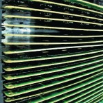
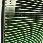
XPC, though softens much more than even FR-1 in the case above, still came out flat post-reflow than when soldered at SAC305 settings. The two racks in the photos clearly show this difference. Current FR-4 laminate applications and products can be evaluated as possible cost reduction candidates. Many consumer products fall into this category where implementing low temperature processing is a benefit.
Just the reduction in capital investment moving away from solder bars & the volatility of metal prices was enough impetus for many to switch over to low temperature soldering. For those that has converted their wave soldering to low temperature SMT, a whole new range of benefits has opened up, from cycle time reduction, through quality improvement to energy, floor space and labor savings.
Low temperature conversion
There are several strategies in converting to low temperature from wave soldering. In early attempts & still in use today, Paste-In-Through-Hole (PITH) extrudes paste all the way into PTHs as in the preceding picture. Sometimes employing unconventional processes such as nozzle printing, this approach; when combined with component & other optimizations, addresses many hole fill issues that usually plague wave soldering. Printed either on top or bottom side, PITH leaves the least residue of the few approaches discussed here. Another approach is to simply overprint, then relying on the surface tension of molten solder later on to form proper solder joints. Although the least complicated & most straightforward, there must be sufficient clearance around each PTH location. It should be pointed out that there could be unacceptable flux residue footprint post solder over the solder mask, depending on quality criteria or electrical performance.
Finally, a fresh approach that not only addresses various shortcomings of the previous two approaches is a combination of PITH & solder preforms. This means strategically placing solder (in the form of common T&R chip components) by P&P machine over PITH locations. It’s most flexible from the application standpoint & fixes even complex issues that wave soldering normally cannot easily overcome – hole fill of thick, multilayer laminates without excessive flux residue on the bottomside to interfere with pin testing.
Perform benefits
Adding solder preforms takes care of another growing issue – component density. Multiples of small preforms can be strategically placed within tight quarters to employ PITH & yet still satisfy hole fill & fillet requirements – consistently. Paste printing & preforms are more precise than wave soldering, resulting in repeatable hole fill & fillets even in thick, multilayer, high thermal mass assemblies. The high thermal shock of extreme wave soldering settings is also avoided altogether for such critical & expensive assemblies.
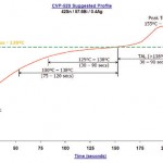
Aside from obviating the high thermal shock of assemblies contacting molten solder at the wave, low temperature reflow only exposes assemblies briefly to temperatures above 138°C. Temperature rise to peak is typically very gentle in low temperature reflow, as opposed to a sudden & rapid temperature spike in wave soldering. As a result, almost no fixturing / pallet is needed to counteract the effects of high thermal shock.
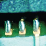
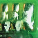
Of the few low temperature alloy choices, BiSnAg has been most popular & proven over recent years. Melting at 138°C, it’s even lower than SnPb but has the advantage of being Pb-free. Given a quick reference of commonly used soldering alloys. Note the difference between BiSnAg that is primarily discussed in this article; as opposed to straight BiSn, which tends to form brittle joints & is the source of much previous bad publicity. For all practical purposes, 57.6Bi42Sn0.4Ag can be taken as eutectic. Low temperature solder usually spread & climb very well for Pb-free. Such fillets tend to be very smooth with excellent wetting on many component termination finishes as seen in the examples of QFN, Piggyback card, SOIC and button cell battery holder.
Strong solder joints
In addition to looking good, low temperature solder joints are strong. Although sometimes stronger than typical SAC305 joints, its been the norm to at least match conventional Pb-free joints in drop-in comparisons. Mechanical strength comparison data in the following should allay fears of very weak joints & correct the historical bad reputation that straight BiSn had created. Solder interaction with both Hi & Lo Tg laminates are shown. Regular production assemblies were randomly tested for the comparisons at left. CVP-520 is a popular low temperature while OM-338PT is a widely used Pb-free solder paste. The stiffer high Tg lost out to the lower Tg laminates, possibly due to more give in the latter during testing. However, the data is consistent between laminate Tg & also alloy processing temperature.
With data already available & the potential cost benefits, low temperature processing should be considered for implementation where suitable. There is even a software out there called Aspen to take the guesswork out of low temperature implementation. So join in this exciting alternative as even more promising developments are already in progress & more lie ahead!
http://alpha.alent.com/
Zusammenfassung
Das Löten im SMT-Prozess mit niedrigen Temperaturen könnte ein Schlüsselfaktor dafür sein, um enorme Kosten bei Komponenten und Laminate zu sparen. Denn wenn der teure Wellenlötprozess so ersetzt werden könnte, werden nicht nur kürzere Prozessabläufe erreicht, sondern auch Energie eingespart und auch die schädlichen Effekte des thermischen Schocks abgeschwächt, wie der Artikel aufzeigt.
Le brasage dans le processus TMS à basses températures pourrait être un facteur clé pour réaliser d’immenses économies dans le coût des composants et des stratifiés. Car si l’onéreux processus de brasage à la vague pouvait être ainsi remplacé, les séquences de processus plus courtes pourraient être obtenues de même que des économies d’énergie ainsi qu’une atténuation des effets nocifs du choc thermique comme l’indique l’article.
Share:
