The ability to non-destructively test semiconductor devices during their manufacture and assembly on printed circuit boards has become ever more important for verifying product quality without compromising productivity. The use of X-ray inspection not only provides a non-destructive test but also allows investigation of optically hidden features such as wire bonds and the quality of post reflow solder joint integrity. During X-ray inspection, devices are exposed to ionizing radiation by high energy photons thereby receiving a radiation dose. Certain semiconductor devices such as dynamic random access memory (DRAM) can be susceptible to damage by high levels of ionizing radiation. This susceptibility may require the user to consider the radiation dose being given to these devices during the X-ray inspection process to ensure that critical thresholds are not exceeded.
Dr. David Bernard, Nordson Dage
Recent commentary has raised the issue of the radiation dose given to electronic components during X-ray inspection. Radiation dose is defined as the amount of energy deposited into the unit mass of the material of interest with the units of radiation dose expressed in Gray (Gy) where 1 Gy = 1 joule/kg = 100 rads. The term dose rate is typically used to indicate the dose per unit of time expressed as Gy/minute or rad/minute that a device will experience at a given position from a radiation source such as the X-ray tube within an X-ray system. Very large radiation doses, many orders of magnitude greater than can be achieved during X-ray inspection, deposit a large amount of energy into the silicon die which can cause physical damage to the device resulting in failure.
Radiation effects
For the manufacturer and user of semiconductor devices, the danger of the radiation dose imparted during X-ray inspection in not this type of gross failure since high dose levels cannot practically be achieved during shop floor X-ray inspection. Instead the potential concern is for more subtle failure mechanisms such as bit flips, loss of program, erase margin or leakage where failure of the device has some statistical or random chance of occurring. The difficulty with these random failure mechanisms for commercial-off-the-shelf semiconductor devices is that their appearance occurs at radiation doses that are orders of magnitude less than what is defied as the ‘gross failure’ variety and therefore potentially within the doses experienced during X-ray inspection.
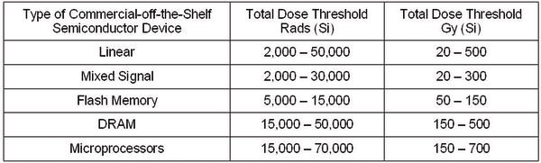
Before concluding that all commercial-off-the-shelf semiconductor devices are at threat from X-ray inspection it should be noted that while some devices are more susceptible to radiation dose than others, the vast majority will not be affected by radiation levels experienced during X-ray inspection. While maximum radiation figures stated in semiconductor manufacturer’s literature vary widely (Table 1), users should consider that actual threshold radiation dose levels for random events are very difficult to define.
It should be remembered that the definition of a random effect means that if the dose threshold is exceeded subsequent failure is never certain in an individual semiconductor device. Exceeding the dose threshold only increases the probability of a failure occurring within an entire production run.
X-Ray Fundamentals
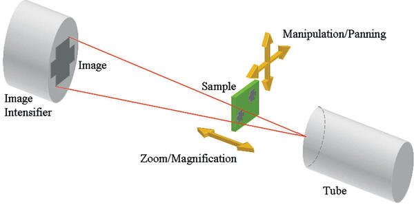
X-ray inspection systems are basically X-ray shadow microscopes where X-rays produced by a tube pass through a sample and into an X-ray image-capture device or image intensifier (Figure 1). The differing materials within the sample absorb more or less of the X-ray radiation depending on their density and atomic number and cast a shadow of that material onto the detector. The closer the sample is moved to the X-ray tube the larger the shadow becomes which is how magnification is achieved.
Factors that affect the dose given to a sample during X-ray inspection include: the distance of the sample from the source of the X-rays, the X-ray power used measured in kilo volts (kV) and tube power or watts (W), the presence of filters of X-ray absorbing material placed between the tube and sample, and repeated inspection cycles. The radiation dose rate varies with the ‘inverse square’ of distance. For example if the distance is doubled from where an initial dose rate measurement is taken, the dose rate will decrease by a factor of 4 from the initial value.
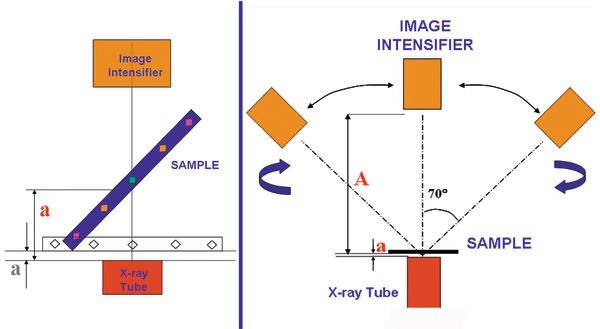
Oblique angle viewing is an important capability of X-ray inspection systems particularly for investigating ball grid array (BGA) and other area array devices since the shape of the solder ball obscures examination of the actual joint interface. Some X-ray systems use an older method of tilting the sample to provide angled views which requires the sample be moved away from the tube focal point thereby reducing magnification. Because continued shrinkage in device size necessitates higher magnification, the preferred method is to keep the sample perpendicular to the focal point at all times and achieve oblique views by moving the detector (Figure 2).
In this manner, the need for oblique views does not compromise the available magnification and potentially limit analytical detail. However, this means there is no net dose rate reduction from having an angled beam at a larger distance from the device so dose estimates must be adjusted accordingly.
Minimizing Radiation Dose
A semiconductor device will always experience some dose rate during the entire inspection sequence however, it is only the time at which it is inspected at the highest possible magnification that is likely to contribute the majority of the dose. Practical suggestions for minimizing the radiation dose experienced during X-ray inspection include consideration of modifying the inspection procedure as follows:
- Increase the distance between the sample and the X-ray tube focal point by raising the board further away from the X-ray tube during inspection.
- Minimize the inspection time by automating the procedure as much as possible so that only those areas that need examination are investigated or inspect critical devices at a lower magnification.
- Consider the necessity of subsequent or repeated inspections such as after rework and repair.
- Make corroborative dose measurements using thermal luminescent detector (TLD) material to validate the understanding of a particular X-ray system confirming the doses that are likely given.
- Place filter material between the sample and the X-ray source. Zinc foil of 100 micron thickness will reduce the dose by a factor of 100 times without greatly compromising the image quality.
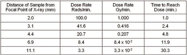
Most importantly the distance from the sample to the X-ray source is one of the most critical factors to the dose rate since it varies according to the ‘inverse square’ law (Table 2).
Changing the focal point distance affects the dose rate that a sample receives and also influences the magnification of the final X-ray image. For example, if the focal point distance used for inspection purposes was increased from 2.0mm to 6.9mm, the analytical information would be hardly compromised but the dose rate as measured at the sample would be reduced by 90%.
Additional Considerations
Gallium arsenide (GaAs) based semiconductor devices are much less radio sensitive than silicon based devices. Silicon is a light metal and as such does not readily absorb higher energy X-rays but is susceptible to low energy X-rays which cause the majority of ‘radiation dose effects’ previously discussed. Radiation dose to silicon is cumulative. Repeating an inspection sequence therefore doubles the dose a silicon based semiconductor device receives. However, board material and thickness as well as device packaging materials and copper ground planes within the board will produce a ‘shadow effect’ that will reduce the actual dose to the active silicon device.
In cases where DRAM devices exhibit random failure mechanisms as a result of a high radiation dose, an independent study indicates that baking the devices for a period of 48 hours at 150 ºC can ‘thermally anneal’ the characteristics of the degradation mechanism recovering the devices to pre-radiation levels. Though baking does improve degraded refresh characteristics of DRAM devices, it should be noted that it may be impractical to facilitate baking after their assembly onto a printed circuit board.
Award winning X-Ray systems
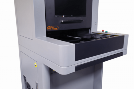
Nordson Dage’s award winning X-ray inspection systems have been specifically and ergonomically designed for the circuit board (PCB) and semiconductor industries offering high resolution nano-focus X-ray systems not only within failure analysis laboratories but also within the production environment. The unique Dage NT sealed-transmissive type of X-ray tube is at the heart of the Dage NT X-ray inspection systems. It supersedes and out-performs the closed and open tube types that are available in earlier systems. The sealed-transmissive tube is the only way to genuinely improve X-ray image resolution whilst still providing true high power and without compromising the resolution and magnification. An example is Nordson Dage’s Flagship system XD7600NT100HP featuring the all new XiDAT 3 detector and the award winning 3rd generation nano-focus Nordson DAGE NT tube. The system also benefits from active X-ray image stabilisation, easy to use point and click software and 70 degree oblique angle views for 360 degrees around any point in the entire inspection area. The unique Dage NT sealed-transmissive type of X-ray tube, the heart of the XD7600NT100HP X-ray inspection system, supersedes and out-performs the closed and open tube types that are available in earlier systems. The sealed-transmissive tube is the only way to genuinely improve X-ray image resolution whilst still providing true high power and without compromising the resolution and magnification. Some features are: 2,000 X Geometric Magnification (12,000 X system magnification), Easy Collision-Free, High Magnification Inspection – even at oblique angle views, Maximum Board Size/Inspection Area – 20“ x 17.5“ (508 x 444 mm) without oblique views.. A vertical system configuration with the X-ray tube sitting below the isocentric ‚move and tilt‘ of the detector, provides the collision free, high magnification inspection required for today’s inspection tasks. Active anti-vibration control, through air suspension, ensures the necessary optimum image stability. A secondary monitor is provided for additional software functionality, such as automated Head in Pillow (HiP) analysis and a large navigation map display, or used as an extended desktop for displaying work instructions and many other applications.
Summary
In certain cases the radiation dose given to semiconductor devices during X-ray inspection may be greater than expected because of the need for inspection of complex packaged devices at higher magnification. Because of this it may be necessary to question if any of the devices being inspected are susceptible to random radiation damage at dose levels greater than their recommended threshold levels. If this is the case, consideration should be given to measuring the radiation dose to be delivered during the proposed inspection regime and taking the necessary actions to reduce the imparted dose during X-ray inspection.
SMT/Hybrid/Packaging Booth 7-226
Zusammenfassung
Der Einsatz der Röntgen-Inspektion ermöglicht nicht nur die zerstörungsfreie Prüfung, sondern auch die Bestimmung optisch nicht erkennbarer Eigenschaften wie Drahtbonds und die Qualität der Verbindung nach dem Reflow-Löten. Während der Röntgen-Inspektion können empfindliche Bauteile wie DRAMs aufgrund zu starker ionisierender Strahlung zerstört werden. Der Anwwender muss daher sicherstellen, dass die Strahlungsdosis den entsprechenden Grenzwert nicht überschreitet.
Le recours à l’inspection par radiographie permet non seulement un contrôle non destructif, mais aussi la détermination de caractéristiques que la méthode optique ne peut pas détecter, telles les soudures au fil, ainsi que la qualité de la liaison après les opérations de soudage par refusion. Au cours de l’inspection par radiographie, les composants sensibles tels les modules DRAM, risquent la destruction s’ils sont soumis à un rayonnement ionisant trop fort. L’utilisateur doit donc s’assurer que l’intensité du rayonnement ne dépasse pas la dose limite fixée.
References
– Bernard, David and Blish, Richard, „Considerations for Minimizing Radiation Doses to Components during X-ray Inspection,” IEEE Proceedings 28th International Electronics Manufacturing Technology Symposium, July 2003
– Ditali, Akram, Ma, Manny and Johnston, Michael, „X-Ray Inspection Induced Latent Damage in DRAM,” IEEE Proceedings 44th International Reliability Physics Symposium, March 2006
Share:


