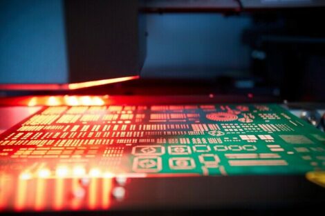
More rapid, more compact, more complex– daily routine in a modern electronics production. The demands on electronic systems’ performance with parallel decreased energy requirements, reduced system size and low costs, define current trends. In search for space-saving contact opportunities in electronic circuits new component types with hidden contact faces have constantly been emerging. Thus, combined with double-sided equipped placement, compact and high-performance assemblies can be produced. But this trend also puts new challenges to test and inspection technologies.
Goepel electronic, Jena (Germany)
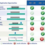
Hidden solder joints can only be evaluated by ‘looking though’ a PCB. The X-ray inspection technology comes in where conventional AOI systems find their limits. 2D x-ray systems are not set to inspect double-sided equipped PCBs. Such systems‘, inspection images show solder joints of both assembly sides as superimposed. Consequently, a detailed process-reliable evaluation is impossible. 2.5 D inspection technology fits better but not ideally. In this case, an angled PCB X-ray, dependent on radiation angle and PCB thickness, enables a separation of the assembly top and bottom sides’ solder joints. If component placement on the PCB is highly compact, a simple angle X-Ray is not sufficient any longer. Similar to the 2D technology, superimpositions occur disabling the safe evaluation of the solder joint.
Separation by digital tomosynthesis
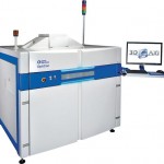
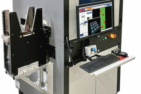
Goepel electronic’s OptiCon X-Line 3D x-ray inspection system works on the basis of digital tomosynthesis. It enables the constant PCB X-ray capturing from several different angles. Captured 2D images are transmitted to 3D data by an algorithmic reconstruction. In this manner, a separation of PCB top and bottom sides’ solder joints is possible free of superimpositions enabling even high density placement inspection. Similarly, superimposed and electrically connected assemblies of so called package-on-package construction can also be inspected. The 3D reconstruction layer-by-layer enables a separation of top and bottom packages and succeeding image processing evaluation.
Enabling fast test program generation
Well-proven in production lines, the OptiCon X-Line 3D’s software and hardware concept provides all the inspection images calibrated to grey value and correct geometry. The geometry true PCB layer reconstruction allows for the utilization of a consistent component library, resulting in a significant reduction in test program generation effort. Hence, users are able to generate a test program by means of CAD data and component entries in the library within shortest time.
PCB warpage compensation
A true to height reconstruction of PCB layers in which solder joints are situated is a prerequisite for solder joint analyses. A 3D x-ray inspection (AXI) system must detect and compensate for PCB warpage, waved surfaces or skewed components because such situation may lead to. For example, if PCB warpage is not spatially compensated, the algorithms test in the wrong solder layers, which may lead to false calls or even escape. GOEPEL electronic GmbH utilises a purpose developed method, which detects and compensates PCB sag during the inspection process. The result is a true to height solder layer reconstruction for a high-quality evaluation of solder joints. Based on PCB condition it is possible to select whether the entire assembly or each partial circuit of a value should be compensated. For PCB warpage determination, a laser triangulation sensor can be applied. It is also possible using software algorithm’s to compensate for PCB sag directly in the recorded images.
Inspection of double-sided equipped BGA components
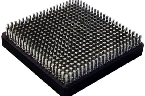
The3D x-ray inspection system OptiCon X-Line 3D of the company enables a safe quality control of solder joints on opposed mounted BGA components, e.g. in double-sided equipped DDR-RAM modules. In the inline production process, single-sided and double-sided equipped PCBs can be inspected within one test run. After image capturing from different directions and succeeding reconstruction, OptiCon X-Line 3D provides the opportunity to analyse both the top and bottom sides of the boards and all layers in between layer by layer. Initially, each BGA solder ball is localised in x/y-direction as well as z-direction. Subsequently, relevant parameters of each solder joint are determined in three layers. By comparing these measured values open solder joints and wetting defects can de safely detected. Additionally, voids can be determined in size and their z-position within a solder joint. Naturally, the system is able to detect solder connections at IC pins and 2-pin components as well as THT components.
The OptiCon X-Line 3D is unrivalled worldwide by utilising the revolutionary GigaPixel image technology. A real-time multi angle image recording is the basis that enables a test speed of 40cm²/s for full 3D PCB capturing.
Zusammenfassung
Der Trend zu immer kleineren und komplexeren Baugruppen beidseitig bestückter Leiterplatten stellt die Inspektionstechnologie vor neue Herausforderungen. Der Artikel stellt ein In-Line AXI-System für die High-End-3D-Inspektion in der Großserienfertigung sowie der Qualitätssicherung komplexer und hochwertiger Baugruppen vor, welches diesen Anforderungen bereits voll entspricht.
La tendance à réaliser des éléments de construction toujours plus petits et plus complexes équipés de circuits imprimés des deux cotés, place la technologie de la vérification face à de nouveaux défis. L’article présente un système AXI In-Line pour la vérification High-End en 3D dans la fabrication en grande série ainsi que pour la garantie de qualité des éléments de construction complexes et de grande qualité qui répond déjà totalement à toutes ces exigences.
Share:
