Nowadays semiconductor technology is displaced in shorter time periods through the next generation. The innovations consist of mostly performance enhancements, stronger miniaturization, higher complexity, rapid increase of integration degree and optimizing costs and quality of the microchips. The choice of an adequate technology in chip wiring is of great importance to satisfy these functional requirements in the future. Here is the screen-printing process of the polymer thick-film technology (PTF) of interest – especially economically – for the development of planar structures.
Regarding the print materials it is very flexible and suitable in applying different materials for electrodes, isolation- and other functional layers side by side or in multilayer structures. Qimonda has tested a process for a novel wafer level package, where conducting paths and isolation layers will be printed in co-operation with TU Dresden. Here polymeric pastes displaces the usually in thin-film technology generated dielectric and conducting structures.
Polymer thick-film technology
Polymer thick-film technology is implemented in the production of electronic circuits since the 50’s. It was primarily used in the production of cost-saving hybrid-circuits. However the used materials in the past did not match the now common specifications regarding thermal properties and migration behaviour. Nowadays the following polymeric paste systems have established:
- Touch-membrane in key pads
- Printed coils in RFID systems (Smart Label)
- Creation of conductor lines on rigid and flexible substrates
- Integrated polymer thick-film resistors
- Filling materials for through holes (Via-Plug)
- Repair of PCB’s
- Development of electromagnetic shielding
The requirements regarding resolution, material cleanness and reliability are unlikely higher for a wafer level package. Polymeric pastes consist of curable synthetic resins in difference to glass or ceramic frits of conventional thick-film pastes. We have a curing process on comparatively low temperatures in difference of the necessary firing process. The electrical parameters in these pastes are determined through different active ingredients. Thus, we can produce conducting, resistance and isolation structures with them.
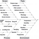
The structured application of the polymeric thick-film pastes usually occurs in screen-printing. The print paste is applied through the openings of the screen material onto the substrate during print process. Hereby, variable print parameters are the snap-off (distance between screen and substrate), the squeegee velocity and the squeegee force. Optimal print results require the adaptation of these print parameters (figure 1). Mesh count, material kind, screen tension, print structure, squeegee hardness as well as viscosity and thixotropy of the used pastes (both sizes are independent of temperature) have great influence. The paste has to be left in room temperature for 5 to 10 minutes after the print and thereby induced irregularities elapse from the screen structure. Part of the fluid solvents evaporate during this “balancing” and afterwards the rest of the solvents is driven out through a 5 to 30 minutes heat treatment (120 to 180 °C) during curing of the polymeric matrix. The polymeric thick-film technology is marked through following advantages:
- Fast, additive process
- Efficient drying process (short with low temperature)
- Cost saving production
- Small material costs
- Environment friendly
- Great variety of substrate materials
- Multilayer ability
- Possible integration of passive components
Nevertheless disadvantages in comparison to the printed board technology, the thin film technology or the conventional thick film technology cannot be disregarded, for instance:
- Lower conductivity,
- Greater structure sizes and
- Smaller abrasion resistance.
Screen-printing: Testing of the fine line ability
While the minimal line width of thick-film circuits was 120 to 200 µm 10 years ago, one now is capable to reduce line width to fewer than 100 µm. Line widths with a pitch fewer than 120 µm are necessary for a wafer level package because of always increasing requirements regarding the number of chip connections. Today we already find thick-film circuits with line resolutions smaller than 30 µm in Asia. Hereby it is primarily about components in LTCC technology (Low Temperature Co-fired Ceramics). The conducting pastes are printed on unsintered ceramic foils, which ease the release of the paste from the screen through its ‘absorbing’ surface. In difference to that we are confronted with hydrophobic passivation surfaces in the realisation of a wafer level package. For testing of the fine line printing we analysed different silver based polymeric pastes from many producers in regards to its applicability for the chip-packaging. Previous research and our own tests had shown that polymeric conducting lines have a 10 to 100 times higher square resistance than the according bulk-material. Furthermore, these tests showed that oxidation of particles on polymeric pastes keeps going even after hardening. Copper oxide works as isolator while silver oxide has almost the same specific resistance as pure silver. Thus we passed on testing polymeric copper pastes from the start.
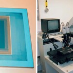
For the characterization of the polymeric pastes glass substrates were printed with a so called trampoline screen, as shown in figure 2. Trampoline screen are mostly applied for precision prints with print resolution # 100 µm. Theses screens are covered with polyester tissue on the outside and with high quality steel wire tissue according to the requirements on the inside. Trampoline screens hold its tension over some 10,000 print movements and can be distinguished through its accuracy # 20 µm and high durability.
Print quality depends on the release of the pastes
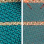
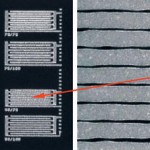
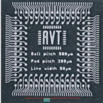
In the results of these first analyses we were able to select adequate pastes and determine the print parameters. It was proven that structure widths of 50 µm and structure spaces of 70 µm are possible with silver filled polymeric pastes and polymeric dielectrics. However these tests show that the release behaviour of the paste is an essential step in assuring print quality. As figure 3 shows, the only few micrometer large meshes of the screen are slightly afflicted through the relatively big silver particles, whereby structures of the screen emulsion can not be completely reopened. Thus, it can happen that already the second print is defective and the screen has to be cleaned before every new print. This problem could be solved through the use of new paste, which had characterized itself through a particular low particle size of 300 µm and a filler material part of 80 mass percentages. We could not assess any changes in print quality in many, consecutive following printing steps with print stops up to 30 minutes. This paste especially developed for the print of redistribution layers builds a smooth and homogenous surface that shines metallically after curing (200 °C, 30 minutes). We were able to prove with the first print tests that pitches of approximately 75 µm can be realised with this paste. The print structures have high angle stability. The paste elapses after the print by 15 µm, which can be observed in the layout development. The layer thickness depends on the structure width to be printed and is between 5 and 15 µm. Figure 4 shows what high print quality could be achieved with the difficult combination of relatively large conductor lines with very low spaces at the same time.
Soldering with low melting pastes and wire bonding
We did soldering and bonding tests to get compatible packaging processes for the fine line paste. The usual lead-free solder pastes (SnAgCu, 218 °C) cannot be applied for silver polymeric pastes because of its temperature limitations. Low melting solders like SnBi (138 °C) offer a good alternative. Figure 5 shows soldering examples on printed silver paste. The solder has completely wetted the printed surface on the pad after remelting. The two X-ray pictures illustrate the necessity of determining the soldering parameters. Without optimization voids will arise and zones with leaching respectively (figure 5, right).
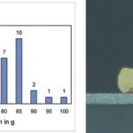
We tested the possibility to bond by using gold wire due to the excellent layer attributes of the paste. In doing so it showed that the ball bond on the tested silver polymeric-paste layer held up, while the wedge bond did not. But it would at least be possible to get stud bumps and to bond from the polymeric silver pad to the chip pad. In spite of different shear types in bond tests we obtain the minimum shear strength. We could determine medial shear force of 73,20 g (minimum: 43,03 g, maximum: 95,33 g) during first shear tests on 36 stud bumps. We had two kinds of shear types through testing (shear through the bump and pulling down of the bump). Hence the span width of shear values is relatively large and does not satisfy production requirements (figure 6). As a result more tests for the bond characteristics and process optimization are necessary.
Conclusion
The thin-film technology usually used for the redistribution layer can be displaced especially for low-cost applications. It was possible to produce functional patterns with line widths of 50 µm and minimal path distances of 25 µm on wafers with a diameter of 200 mm (figure 7). Running, promising test series should reduce the printable structure width to 30 µm. In addition, we need further optimization of screen structure and print parameters.
EPP 451
Share:
