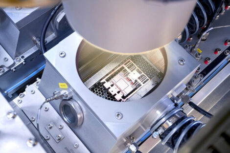
Fueled by the need for faster processing times and smaller device footprints, DEK has developed a next-generation equipment and tooling package that enables the coating of wafers with ultra-thin die attach materials down to 25 microns in thickness.
Traditional dispensing methods and paste die attach processes have manufacturing challenges such as the inability to achieve emerging UPH (units per hour) requirements, limitations on chip footprint due to chip fillet formation and resin bleed and inherent quality and reliability issues that result from insufficient or uneven adhesive coverage. The new system effectively eliminates these issues, allowing the high-speed, high-accuracy uniform deposition of die attach materials as thin as 25 microns with tolerances of ±7 microns using a printing process.
The backside wafer coating process enables ultra-thin, precise deposits of die attach adhesive at high speed with a highly-accurate and flexible screen printing platform. With this method, bondline thickness can be controlled to customer specifications, fillet control is consistent with that of traditional film products without the 20 to 30 % higher cost, UPH is exponentially higher than that of dispensing and the coated wafer can be pre-manufactured and stored until required.
Other significant advantages include the elimination of the fillet and subsequent reduction of paste adhesive volume, improved inventory control and streamlining the supply chain by requiring only one paste formulation for various process needs.
The process can be used for all wafer-level coating processes including epoxy and wafer-level protective backside coatings as well.
EPP EUROPE 421
Share:


