Homepage » Technology » Applications »

Laser Direct Structuring for In-House PCB Prototyping

Applications
Laser Direct Structuring for In-House PCB Prototyping

Laser Direct Structuring for In-House PCB Prototyping
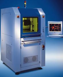
The LPKF Protolaser 100 system is specifically designed for the in-house production of high quality RF and microwave boards. This Protolaser uses a focussed laser beam that isolates the tracks in the copper layer and structures the circuit layout. The residual copper is removed at a speed of up to 1 square inch (6 cm2) per minute without damaging the substrate. With the Protolaser 100 complex prototype PCBs are produced through a completely chemical-free process. It works with tracks as narrow as 50 µm and with the highly precise track edges that are critical for HF circuits.

With its extremely high precision, the Protolaser 100 can process a wide range of circuit substrates including FR4, RT/duroid, and Alumina. The system utilizes a vacuum fixture to secure boards in place.
EPP EUROPE 430
Current Issue
Titelbild EPP EUROPE Electronics Production and Test 11
Issue
11.2023
READ
Newsletter

Subscribe to our newsletter now

Webinars & Webcasts

First hand technical knowledge

Whitepapers

Find all current Whitepapers here

Videos

Find all current videos here


Industrie.de Infoservice
Vielen Dank für Ihre Bestellung!
Sie erhalten in Kürze eine Bestätigung per E-Mail.
Von Ihnen ausgesucht:
Weitere Informationen gewünscht?
Einfach neue Dokumente auswählen
und zuletzt Adresse eingeben.
Wie funktioniert der Industrie.de Infoservice?
Zur Hilfeseite »
Ihre Adresse:


Die Konradin Verlag Robert Kohlhammer GmbH erhebt, verarbeitet und nutzt die Daten, die der Nutzer bei der Registrierung zum Industrie.de Infoservice freiwillig zur Verfügung stellt, zum Zwecke der Erfüllung dieses Nutzungsverhältnisses. Der Nutzer erhält damit Zugang zu den Dokumenten des Industrie.de Infoservice.
AGB
datenschutz-online@konradin.de