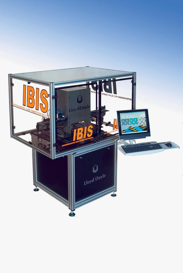
Lloyd Doyle has showcased the IBIS system, a new development for solder bump inspection at Productronica. IBIS, the Interferometric Bump Inspection System, uses emerging technology to offer production volume solder bump inspection on chip carriers. It is designed to inspect and report on the position, height and shape of solder bumps on the die-attach side of chip carriers, ensuring that the carriers are within specification for chip attachment. The system is designed to inspect coined and non-coined solder bumps on chip carrier die attach regions. It is capable of scanning 3,000 devices per hour and reporting on solder bump height, volume, circularity and co-planarity.
It uses massively parallel digital signal processing technology coupled with true white light interferometry to offer 20 to 30 times improvement over existing interferometry systems previously available. The company’s proprietary enhancements give IBIS the edge for solder bump height measurement. This enabling technology will be transportable to wafer and chip solder bump measurement in the future.
“This system represents a breakthrough in inspecting and measuring bump parameters accurately at high speed,” said Roy Lloyd, CEO. “It will enable manufacturers to have 100 percent inspection of solder bumps on chip carriers rather than only being able to measure these under laboratory conditions.”
EPP Europe 438
Share:
