The increasing functionality and decreasing size of today’s consumer electronics has led to the development of the package-on-package (PoP) technology. Using PoP devices allows designers more flexibility and decreases the development time and cost. From the assembly system point of view, PoP requires new techniques when compared to standard SMT assembly.
Gerry Padnos, Juki Automation Systems, Morrisville (USA)
One problem is how to get the devices in a stacked assembly to reflow. Flux or specially designed dippable solder paste must be applied to the components before they are placed. The application of flux or solder paste is not common for standard SMT assembly so additional hardware and software on the assembly system are required. The next challenge is the requirement to place the components on top of each other. Of course every machine has some up and down, or Z, movement, but the ability to stop at varying Z heights depending on the placement location requires additional hardware and software also. Some PoP devices are a simple stack of identical components while others are different components in a specific sequence. The assembly process must have software that identifies the layer for each component and prevents components from being placed out of sequence.
Assembly methods
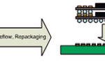
The two main methods of PoP assembly are “pre-joined” and “on-the-fly”. The pre-joined method of assembly uses a two pass process. In the first pass, the devices that will be stacked later are assembled. Components are placed onto other devices in a carrier. The entire carrier is then sent through reflow to join these parts. The now pre-joined devices are then re-packaged for picking by the assembly system. These devices are returned to the placement machine to be stacked on top of each other or to be placed on top of a different device. The on-the-fly method is where the all layers are placed and the complete stack is reflowed all at once. The first layer is placed on the PCB or carrier directly and additional layers are placed successively. After all components have been placed in the proper sequence, the entire assembly is reflowed. The first layer is often attached with normal solder paste printing, but dippable solder paste or flux can also be used. It is important to use the same flux medium in the solder paste and the fluxer to ensure compatibility of the reflow profile. The pre-joined method reduces some complexity for the placement machine, because each step is more like traditional SMT assembly, but adds handling and other possible concerns.
Before discussing how to assemble PoP, it is important to understand how various types of components are being used in PoP assembly. By building the memory package vertically, designers can add more memory to a device without needing to leave unused space on the PCB when less is required. They need only one set of pads and can install PoP memory with 2 or more vertical layers. Nearly all PoP devices use BGA type balls on the bottom side of each layer as the interconnection. The main difference between a PoP device and a standard BGA from the assembly point of view is that the PoP devices have pads on the top side in addition to the balls on the bottom. The pads are the interconnection between the different layers in the final package. From an assembly point of view, System in Package (SIP) is very similar to PoP. SiP is more often just 2 layers so in some ways it is not different from standard SMT assembly. PoP, on the other hand, is usually used for a device that requires flexibility of more or less modules. One example of PoP is a solid state drive. Increasing the drive size simply requires more modules to be stacked on top of each other. To further complicate things, sometimes several SiPs can be stacked to create a PoP device. The good news is that the assembly system really doesn’t care what its placing, only how it needs to be placed. The PoP stack may be composed of all identical layers or different components on each layer. When the layers are different, the sequence of assembly becomes important since the device will not work if assembled in the wrong sequence.
Fluxing
In the more common PoP assembly methods, one layer of parts is placed on the PCB, but subsequent layers are placed immediately on top of the first layer. It is possible, and common, to print solder paste onto the PCB for the layer one placements, but there is no method currently to apply solder paste to the tops of these parts after they have been placed. The preferred method is to apply flux or dippable solder paste to the balls of layer 2 and higher parts. This must be done on the assembly system since the parts are going directly from their packaging to the PCB. This paper is focused on the assembly process only and will not discuss the merits of flux versus dippable solder paste. From the assembly point of view, the only difference between flux and dippable solder paste is how well they work in the flux unit. Fluxing has been around for many years on different machines on the typical SMT floor, but has rarely been used on mainstream SMT assembly systems. Specialty placement machines designed more for semiconductor placement have also used fluxers for many years. Although the device is often called a “fluxer” or “flux applicator”, the newly developed dippable solder pastes are usually compatible. For this paper, the word “flux” can be considered interchangeable with “dippable solder paste”. The main task of the fluxer is to provide a method of applying a uniform and consistent amount of flux to the components. The design must be such that each component dipped will have a uniform amount of flux across all of the balls or leads. The depth of the flux on the component depends on the diameter of the balls on the component. Typically the depth of the flux should be 40 to 50 % of the ball diameter to ensure proper coverage. If the depth is too much, the flux could touch components on the bottom side and cause adverse reactions. If the depth is too low, there will not be enough flux for proper reflow. There are two main types of fluxers used for SMT assembly systems: linear and rotary. Spray type fluxers used on selective or wave solder machines are not appropriate for the SMT assembly systems. Linear and rotary fluxers are both dip type fluxers where components are dipped into the fluxer one at a time. Both types must have some reservoir or container for the flux and a method to ensure uniform and proper flux application.
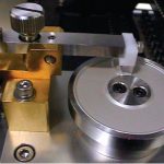
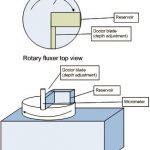
Linear fluxers ensure the uniformity of depth through a sliding plate with a precision cavity milled for the desired component dimensions. The plate slides back and forth under the reservoir to refill and then scrape off any excess. After the component is dipped, the plate slides closed again to refill and to minimize exposure to air. The dimensions and depth of the cavity are fixed on each plate, but the plates can be easily changed for different requirements. Some plate designs allow more than one depth on the same plate, increasing the flexibility of the linear fluxer. The benefit of the linear fluxer is that the depth of the flux is extremely uniform across the entire cavity. It is also more difficult to incorrectly set the flux depth since it is fixed by the plate. Only by choosing the wrong plate for the product could the depth be incorrect. One drawback of this design is that it is more difficult to change the depth when needed compared to the rotary fluxer. Rotary fluxers have a rotating disk that flux is dripped onto. A doctor blade scrapes off any excess to ensure the proper depth of flux. The depth of flux is set by adjusting a micrometer attached to the doctor blade so it is very easy to change the depth of flux. The disk rotation pauses whenever the component is ready to be dipped and then continues again after the dip is complete. The constant rotation is required to keep the depth of flux uniform. One concern with rotary fluxers is that the centrifugal force can make the depth of flux slightly deeper at the edge of the disk than at the center. Rotary fluxers are also usually larger, or have a smaller maximum component size, because the disk has to be more than twice the diameter of the maximum component size.
Placement height compensation and sequencing
Second to the ability to dip devices in flux or solder paste is the ability to compensate for the 3D nature of the PoP assembly. Unlike standard SMT where every part is placed on the same horizontal plane, PoP placement height changes with every different assembly and every layer that is added to the stack. The assembly system must have a way to accurately account for the change in placement height to avoid excessive force on the devices or damage to the machine. The ability to measure and adjust for the Z height variations is what really makes PoP assembly process unique. There are some packages that require fluxing, but not height compensation. PoP requires both.
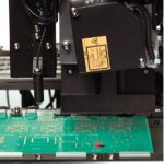
To compensate for the different placement heights, first, the assembly system must have accurate Z control for each placement head. Next, the machine needs a way to measure the actual placement height prior to placing each layer. The best way to do this is using a laser to measure the height of each placement position just prior to placing the next level part. It is possible for the assembly system to calculate the proper placement height based on the PCB height and devices already placed, but measuring each location individually with a laser is more accurate. The laser height measurement sensor is mounted to the assembly system’s placement head. The measurement is performed very similarly to checking fiducials or bad marks. The sequence of placement is also a potential issue for PoP assembly. Some applications have a stack composed of different devices. In these cases it is critical that the devices are placed in the proper order. The assembly system software must have a method to identify which “layer” each device will be placed on and a method to ensure that higher layers are not placed before lower ones. Often in standard SMT, optimization software may rearrange the placement sequence to reduce assembly time. In addition, it is common when an error occurs for assembly systems to continue to place subsequent components. If this happens without software layer controls, an error placing a layer 1 device could cause a layer 2 device to be placed first. The ability to specify the layer for every placement is used to force the optimization software to maintain the correct placement sequence. It also stops the machine if an error occurs on one layer of placements before placing any of the subsequent layers.
Components and assembly
When investigating PoP capabilities, it is important to ensure the component handling capabilities of the assembly system will meet the requirements for assembly. The main thing to keep in mind is the maximum overall height of the final stacked device and not just the height of an individual component. There are several possible assembly methods, each with many possible variations. PoP assembly using pre-joined devices is a multi-step process. This method is more suitable for applications where more than a single component will be placed on each layer; a BGA and some passive components, for example. In the first step, all of the parts are placed on a single layer. Later, these devices will be placed on a stack. Normally the first layer is made on a standard panelized PCB that will be cut apart later, or on individual units placed into a carrier. This first step is identical to standard SMT assembly. No fluxing is required since there is only one layer that can be handled with a standard stencil printer. Height compensation is also not required. The PCB or carrier is then reflowed and cut apart into individual devices which are then put into a packaging suitable for the assembly system to pick from. In the final step, the pre-joined devices are placed onto a stack using PoP methods. Standard solder paste may be used for the first layer. All subsequent layers will have the devices fluxed, the stack height measured, and the device placed. Flux or solder paste dipping is a good method when there is only one component on each layer or when there are only two total layers. This method requires less overall processing and handling of devices. Fluxing adds processing time to each placement in order to dip the component and is in addition to the normal pick/center/place time. This is why this method is not really recommended for devices with more than a single component on each layer. The flux dip method is very straight forward with only two steps added when compared to traditional SMT assembly. 1. The base layer is screen printed with solder paste. 2. Layer 1 devices are placed. 3. The height of each placement location is measured. 4. Layer 2 parts are picked, fluxed and placed. 5. Steps 3 and 4 are repeated for each additional layer. One common variation to this method is to replace the solder paste printing of layer one with flux dipping. This completely eliminates the need for the stencil printer in the production line. The production time will be increased but this can be weighed against the potential cost and programming savings. Generally, the placement accuracy for PoP should be the same as other similar BGA components on any given machine. One method to improve the placement accuracy is to use fiducials for each layer of placements. The need for using fiducials is completely dependent on the application and machine accuracy. Since devices are placed on top of each other, there is a possibility of tolerance buildup from the devices as well as the assembly system. Fiducial marks can be designed onto the top of each layer that can then be used for higher layers. If it isn’t possible to add fiducials, many assembly systems have pattern recognition functions that could use the pads on the top of the components as fiducials. Since these pads do not have any solder paste on them, the accuracy should be quite good. The handling of this function by the assembly system is identical to local fiducials on traditional SMT assembly. This means fiducials must be defined for each layer of devices. Before the next layer is placed, the fiducials on the previous layer are checked. The main restriction using this function is that most assembly systems have fixed focus fiducial cameras. The ability to assemble PoP devices requires two main changes from the standard SMT assembly process: application of flux to some or all components and the ability to stack components on top of each other. While these two requirements are new to the SMT assembly process, the technologies and hardware have been around for many years and are well established. There are several possible assembly processes that can be used depending on the specific application. Adding the ability to assemble PoP devices is not difficult after understanding the basic requirements for PoP assembly as well as the specific application requirements.
ZUSAMMENFASSUNG
Die zunehmende Komplexität bei abnehmender Größe moderner elektronischer Geräte hat zur Entwicklung der PoP-Technologie geführt. Im Hinblick auf die Bestückungstechnik erfordert PoP im Gegensatz zur herkömmlichen SMT Bestückung den Einsatz neuer Technologien.
La complexité croissante des appareils électroniques avancés a abouti à l’élaboration de la technologie PoP. Dans le domaine des techniques d’équipement, les systèmes PoP imposent, à la différence du montage CMS traditionnel, le recours à de nouvelles technologies.
Share:
