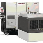
The memory market continues to progress with greater densities and higher volumes and cost is always a top priority for memories makers. T5385 from Advantest delivers the required flexibility allowing the chip industry to choose the configuration that best fits its’ needs. The best tester resource matched to the number of wafer die can be put together. It is possible to change the tester composition matched to the test method such as Full Pin, LPC, DFT, and BIST.
Nunzio Renzella, Advantest Europe (Germany)
Memory chips used in today’s computers and other electronics deliver faster processing speeds, higher data storage and more efficient power consumption than previous generation devices. To enable these gains, the semiconductor industry is aggressively migrating to smaller process that allows more chips and greater densities to be produced from each wafer. Throughput has therefore become a critical issue in memory wafer test, with chipmakers demanding significant increase of productivity.
Advantest’s new T5385 delivers highest test capability and flexible pin configurations that allows tester pin resources to be optimally allocated for efficiency, reduced touchdowns and improved throughput. The T5385 not only boasts an 1536-DUT parallel test capacity using one test head but also delivers 533 Mbps capability for increased throughput and lowered test costs, making it an ideal solution for high-volume wafer-fabs.
The tester can be used to test and characterize general-purpose memories such as DRAM, SRAM and all types of flash memories such as NAND and NOR. The system also delivers Known Good Die (KGD) for consumer devices, Low Power DDR2 (LPDDR2) and DDR3 multi-die and stacked devices. A free tester resource can be set by adopting the site structure and the module structure. One test station is used, which can be configured with a maximum of eight test sites.
Flexible Solution for variety of applications
A test system of the test site type consists of multiple independent test site modules, each equipped with all the necessary functions such as the ALPG, TG, FCSC, driver/comparator, etc. The architecture per site supports flash memory testing. The T5385 boasts a proprietary tester-per-site architecture optimized for flash memory, contributing to reduced test time.
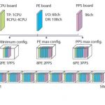
Beyond of that, the T5385 has a modular structure. Each test site is equipped with three different types of modules: CPU, PE (pin electronic) and PPS (programmable power supply). The tester can have different configuration site based on number of PPS boards or PE boards mounted : configurable ratio of I/O vs PPS to match all memory devices.
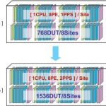
Testing a x4 device (databus of 4I/O) it’s possible to reach 768 duts in parallel per system with 1CPU, 8PE, 1PPS per site, multiplied by 8 sites. Stepping forward a x2 device, it’s possible to increase the parallelism till 1536 duts per system just upgrading it with 1PPS module per site (8 PPS module per system).
Modular system
Designed for engineering use, the smaller T5385ES offers all the functional and performance qualities of the production system. Engineers can easily perform evaluation and characterization, and test programs developed on the tester can be seamlessly transferred to the T5385, accelerating development processes.
The T5385 test system uses FutureSuite operating system software of the company which offers an easy testing programming environment for shorting program development time. It has two different programming language: MCI is a C-like to permit the users to work on C and ATL to keep the full compatibility between all memory testers of the company.
Zusammenfassung
Das DRAM-Wafer-Testsystem T5385 testet bis zu 1536 Bauteile parallel. Neben einer höheren Leistung und niedrigeren Testkosten ermöglicht das Testsystem einen KGD-Test (Known Good Die) für Konsumelektronik mit bis zu 533 Mbps, wodurch sich eine deutlich höhere Fertigungsausbeute erreichen lässt.
Le système de test de plaquettes DRAM T5385 est capable de tester simultanément 1536 composants. Outre de plus grandes performances et des frais de test réduits, le système permet d’effectuer des tests KGD (Known Good Die) pour les produits électroniques grand public jusqu’à 533 Mbit/s. Ainsi, le rendement de production est nettement plus important.
Share:
