There is no shortage of acceptance amongst experts for MID technology. Users also report positive experience throughout. This is not surprising given the many benefits including compact design, lower weight and higher design flexibility. The associated costs are also lower thanks to savings on PCBs and connectors, as well as simpler assembly, testing and service. Nevertheless, mass production in really large numbers is still fairly rare. The main reason for this is that many design engineers still know too little about the parameters involved in the various process steps. This article presents the design rules and requirements involved in the successful realization of MIDs – and shows that they no longer represent any serious hurdle.
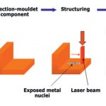
Various methods are available for the production of MIDs (molded interconnect devices). This article looks at the LDS method (laser direct structuring) whose advantages over alternative methods include short process chains, non-destructive processing, fine structural resolution, low production costs, and high levels of environmental compatibility. The method involves three main steps: injection moulding, laser structuring, and metallization, which focuses on the laser technique. Injection moulding is used to turn the granulate into laser-structurable moulded components in a single component injection moulding process. The thermoplastic polymers include a special additive which can be activated by laser light. This laser structuring exposes metal nuclei on the activated surfaces to create a seed-layer on which copper, nickel or gold can be plated during chemical metallization (for example, to produce layers with thicknesses of 8/4/0.1 µm). This creates the circuit artwork. The construction method and connection technology also have to be taken into consideration if the MIDs are to be equipped with assemblies (figure 1).
Manufacturing moulded parts
Injection-moulded MID components are basically made in the same way as conventional injection moulded parts. Standard surface quality is perfectly adequate and therefore no surface polishing is required. Mould release agents should not be used in injection moulding to ensure that optimal results are produced during the subsequent metallization process. The lubrication of ejection pins should also be avoided, or used extremely sparingly. The first step is to select the material to create the injection-moulded part. A number of conventional thermoplastic materials are available containing an additional ingredient. These materials include high temperature nylons, PBT, PET, PPA and LCP as well as a range of PC/ABS polymers.
Selection criteria include the material costs and the technical specifications, because the part must be compatible with the MID application and must for instance, be able to withstand soldering and operating temperatures, be capable of bonding, and have the required mechanical properties. The precise properties of the materials are described in detail in the manufacturer’s datasheets.
High quality moulding of the MID components helps ensure a smooth production process: The shape should be selected to prevent any possibility of mutual rubbing or adhesion when plating the parts by using the drum technique for instance. Tracks can be specially indented at edges to prevent damage. Spacers such as bumps and domes also prevent the parts from sticking together. The parts should also be geometrically designed to ensure that they cannot become entangled in one another or hooked up to one another. De-aeration structures ensure that hydrogen bubbles detach themselves completely during the subsequent metallization process. These bubbles can have a negative impact on the build-up of layer thickness during metallization.
The components have to be fixed in place during laser structuring and assembly. The fixing positions must not harm any sensitive parts such as tracks, contact pads or component seats. Rebates enable cheap universal holders to be used without damaging the activated zones when changing the component’s position and after laser processing. Holding or clamping devices are required during frame metallization in particular. The holding and clamping devices should be made of plastic to avoid the deposition of any contaminants during metallization.
Artwork planning and realization
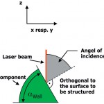
One of the important goals during the development and manufacture of MIDs is the efficient use of space with the finest possible structures. Track widths of $ 150 µm and gaps of $ 200 µm have proven ideal in practice, although thinner tracks and gaps are possible. Mechanical and temperature stress can give rise to tension cracks along the bonding seams in particular. The artwork must therefore not cross any of these bonding seams because this could have a detrimental effect on the tracks (figure 4). To reduce the deposition of the laser ablated material or false plating on the walls, the zones to be subsequently activated should not touch walls directly. The separation for walls with an angle of 45 ° should be $ 150 µm, the separation from steeper walls with angles of 70 ° for instance should be $ 250 µm. An adequate separation between the tracks and ejection pins must also be incorporated in the design. Failure to do this could cause thinning of the track or even a complete break in the track as a result of fracturing or shadowing. The surface of the polymer is activated by the laser light. The maximum angle of incidence of the laser beam on the surface to be structured must not be exceeded if safe activation is to be achieved (figure 2). The angle of incidence is the angle between the orthogonal to the activated surface and the laser beam. Angles of incidence exceeding 70 ° are reduced to less than 70 ° by rotating the component during the laser processing step. This technique can also be used to realize artwork lying on surfaces separated by angles of 90 °.
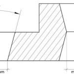
Through-plated holes can be realized by activating the vias by laser light. To ensure that the laser can process the inside walls of the through-plated hole at a suitable angle of incidence, the vias have to be conical on one side or both sides depending on the thickness of the material. In the case of thick walls (figure 3), the internal diameters of the vias must be enlarged to ensure unimpeded processing by the laser beam (aspect ratio of simple cones 1:1; for double cones 2:1). The zone in which the component can be processed is limited by the maximum possible scan field volume of the laser. The scan field of the LPKF MicroLine 3D laser system for instance has a frustrum with a base diameter of 160 mm, a height of 24 mm and a lateral area angle of inclination to the base of 77 °. Copper, nickel or gold are electrolessly plated on the activated surfaces during metallization. Metallization can be carried out using the drum or frame metallization method. The type of component determines the nature of the frames or the mesh width of the drum. It is important to test the activity of the bath under optimal bath loading to guarantee optimal plating, and also to ensure that the components can move around properly, and that filter columns are used for circular filtration of the baths. Each plating step is carried out wet-in-wet taking care to flush properly after each phase.
SMD assembly
The biggest challenge for the SMD assembly of MIDs is the three-dimensional shape of the substrate. To guarantee the freedom of movement of the solder dispenser and the component vacuum tweezers in automatic assembly lines, it is essential to design-in adequate separations between the SMD seating areas and the MID component edges and walls. Components can be placed on flat surfaces located at stepped heights. The slopes connecting these steps should, however, not contain any assemblies, and be exclusively reserved for the connecting tracks.
Quality assurance
Process-optimized equipment is essential to ensure high quality MID production. This also includes regular control, calibration and maintenance of the equipment. The results of laser processing are controlled by for example visible inspection. Automatic optical inspection and in-line activation-level determination methods are currently still under development.
EPP Europe 444
Share:
