The trend towards increasing miniaturisation of microchips is continuing. One key step in the production chain is lithography. In this step, integrated circuit patterns are transferred to a silicon wafer. They mark the places where conductive material is applied in consecutive steps such as etching and ion implantation. The lithographic process is conducted by so called step and scan machines, or scanners. ASML, a Dutch company, is a world market leader for these machines. German optics specialist Carl Zeiss SMT (Semiconductor Manufacturing Technologies) supplies them with optical modules.
Microelectronics is the main drive behind the technological progress of the last decades. With each level of miniaturisation electronic devices not only become smaller, but also more powerful, new applications and opportunities arise. At the beginning of this process in the mid-1960s, electronics pioneer Gordon Moore stated his famous law according to which the number of components in a computer chip doubles every one and a half years. This statement has been valid ever since then and experts judge that it is going to be so for at least ten or fifteen years. Meanwhile, miniaturisation has reached the nanometre level demanding high-precision equipment for the production of microchips. One key step in the production chain is lithography.
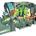
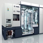
The joint technological achievements of both companies grant their leadership in this very specialised market, where success depends on the amount of miniaturisation the optical equipment can achieve. At the moment, ASML’s immersion technology reaches the highest resolution. The newly developed EUV technology, using extreme ultra violet light, is currently tested in two prototype machines in Belgium and the US (figure 1).
The core element of each lithography platform is its optical column, which consists of an excimer laser light source, followed by an illuminator to shape the beam. Different beam shapes like quadrupoles, ring or circular, are used to optimally illuminate different kinds of chip structures. The pattern mask or reticle that is to be printed on the silicon is inserted between the illuminator and the object lens that is used to scale down the patterns to one quarter of the size on the mask.
Resolution of lithographic stepper scanners follows the formula dmin = k1 · l/NA with dmin signifying the minimum feature size that can be achieved. The main factors that can be influenced by the optical technology are l, the wavelength of the light, and the numerical aperture NA. The second value defines the range of angles over which the system is able to accept or emit light. Consequently low wavelength light and a high aperture are required to reach the smallest possible detail size. The so-called process factor k1 is depending on the detailed processes set up by the chip manufacturer. This factor cannot reach levels below 0.25. However – the lower k1, the more susceptible the whole production process becomes for even least variations of for example laser power, optical aberrations, temperature etc. Standard machines use process factors between 0.3 and 0.5.
Increasing numerical aperture by immersion
The main factor to define NA is the half angle of the light cone between the lens and the focus point on the wafer for air as optical medium between the last lens element and the wafer. Therefore mathematically, NA increases in correlation with the lens radius. In practise, larger lenses accept more light. In order to assure a low level of aberrations (below 1 nm rms) more lenses are applied as well as lenses with aspherical surfaces. Meanwhile, optical lenses of standard lithography scanners consist of an assembly of up to 20 lens elements, the largest of which are over 30 cm in diameter. As a consequence these projection lenses are 1.3 meters high and weigh more than a metrical ton. Carl Zeiss SMT has to coat the various lenses with special antireflective materials. Else there would be so many reflections that hardly any light is left to reach the wafer. These lenses deliver apertures of 0.93, which is very close to the theoretical maximum of 1 for air as a surrounding medium. They reach a resolution of less than 65 nanometres.
With immersion technology, ASML and Carl Zeiss SMT have found a way to increase NA above 1 by changing the surrounding medium. NA increases in proportion to the refractive index of the surrounding medium. While air has an index of 1.0, it lies at 1.44 for pure water at 193 nm wavelength. If the wafer is absolutely covered with a thin water layer during the scanning process, resolution can be reduced to less than 40 nm. To meet this goal, not only the optical equipment had to be considered. Using a liquid as an intermediate layer brought up other challenges. While the wafer has to be covered with a consistent layer of liquid during the scanning phase, not the slightest drop is allowed on it afterwards. Every single drop may cause problems by altering the wafer surface. Not the slightest disturbance on the liquid surface can be allowed. For example, bubbles generated by the wafer moving through the liquid can act as concave lenses that distort the light and ruin the scanning results. Last, but not least, the water has to remain absolutely pure for a considerable amount of time to allow large-scale mass production. To avoid all possible disturbances, the parts of the machine that move and fix the wafer had to be redesigned, as well. ASML introduced the first immersion machines in 2003. Meanwhile, they are used for mass production all around the world.
Reducing wavelength with EUV
The second factor that can be influenced in the optical resolution formula is wavelength. Traditional as well as immersion machines most commonly use Krypton or Argon fluoride excimer lasers emitting ultraviolet light of 193 or 248 nm wavelength respectively. Now microchip lithography takes a big innovative step into the extreme ultra violet (EUV) spectrum with wavelengths around 13.5 nm. This technology is currently tested in two machines located in Belgium and the United States, where ASML customers can gather first impressions.
Caused by the difference in wavelength, the optical technology had to be changed fundamentally. Even with the current UV light, only special materials could be used in the lenses. Only fused silica and calcium fluoride have the right transparency level in this spectral range. There is no optical material that is transparent in the EUV range, though. Therefore, mirrors are used instead of lenses. Because of the short wavelength, thin alternating coatings of molybdenum and silicon are applied to reflect about 70 per cent of the radiation. To bundle the light and avoid diffusion losses, aspherical mirrors are used. Their production is far more complex than that of spherical ones. Because of the short wavelength, their surfaces have to be absolutely accurate and must not allow surface deviations from target above 0.2 nanometres rms.
Another challenge for the optical design is caused by lack of transparency. Unlike lenses, mirrors cannot be arranged in line, but require elaborate arrangements so they do not get into each other’s way and still allow for maximum efficiency.
For ASML’s current EUV model, Carl Zeiss SMT applied six aspherical mirrors to reach resolutions of about 22 nm and beyond. Experts are positive that this technology can be used to produce even smaller details. The company judges that EUV scanners will be available for customer research in 2010. In this phase, chip manufacturers use one machine to align their production processes to the new equipment. Usually this process takes about two years so that volume production of EUV scanners will most certainly start in 2012.
Long lasting business relationship grants success
“In terms of regular printing, our machines would be able to print a map of the Netherlands with a resolution high enough to see every cobblestone on the sidewalk”, says Dr. Robert Jan van Wijk, head of ASML’s Development & Engineering Imaging Department. “You can imagine that high end products like ours can only work with the best functional components. Thanks to our long-time co-operation my colleagues at Carl Zeiss SMT know exactly what we need and their company is renowned for its high standard optical equipment.”
“ASML is our most important customer”, confirms Winfried Kaiser, head of Product Strategy at Carl Zeiss SMT and the first Fellow of Carl Zeiss. “When ASML and Carl Zeiss started the cooperation the lenses we built weighed about 20 kg. Now they weigh up to 1000 kg and both our turnovers have developed in the same proportions. This market is so specific that our companies have developed a kind of symbiotic relationship.”
EPP Europe 450
Zusammenfassung
Die in enger Zusammenarbeit mit der Carl Zeiss SMT entwickelten Technologien ermöglichen die Fertigung immer kleinerer Strukturen auf Mikrochips. Einer der viel versprechenden Ansätze zur Erzeugung dieser Strukturen ist die EUV-Lithografie (Extreme Ultra Violet) und die Immersion, die von ASML in seinen Wafersteppern genutzt wird, um Leiterbahnenmuster auf die Waferoberfläche zu übertragen.
Les technologies SMT développées en étroite collaboration avec la société Carl Zeiss permettent de fabriquer des structures de plus en plus petites sur puces électroniques. L’une des approches prometteuses de la fabrication de ces structures est la lithographie UVE (Extreme Ultra Violet) et l’immersion utilisée par ASML dans ses graveurs à répétition pour imprimer un tracé directeur à la surface de la plaquette.
Le tecnologie sviluppate in stretta collaborazione con Carl Zeiss SMT consentono di produrre strutture su microchip sempre più piccole. Una delle diverse nuove tecniche più promettenti per la creazione di tali strutture è la litografia EUV (Extreme Ultra Violet) e l’immersione, utilizzate da ASML nel loro wafer stepper per trasferire le piste sulla superficie del wafer.
Business co-operation
Since ASML was established in 1984, the company obtains the optical technology for its chip manufacturing machines from Carl Zeiss SMT. This long lasting business co-operation has become a success story for both sides. Together, they managed to reach a 60 per cent share in a market with two other competitors – both of them based in Japan. Even some major Japanese microchip manufacturers now use ASML machines.
Share:
