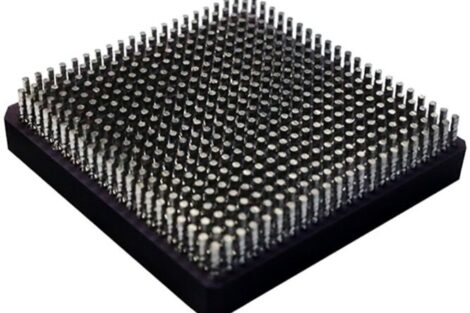
Ball grid arrays (BGAs) have become quite common on printed circuit board (PCB) assemblies, which, in turn, opens up a new world of failure modes and analytical tools/methods required to properly evaluate these components. Traditional style SMT components such as SOICs or QFPs allow for inspection of the solder joints visually to look for anomalies; however, BGAs do not afford this opportunity because most of the solder joints are hidden underneath the components and are not visible to the eye.
Aaron Olson, STI Electronics Inc., Madison, Alabama (USA)
The article discusses some of the failure modes STI’s lab has experienced and the tools and methods used to conduct the investigation.
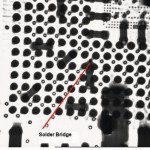
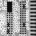
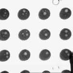
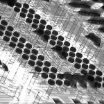
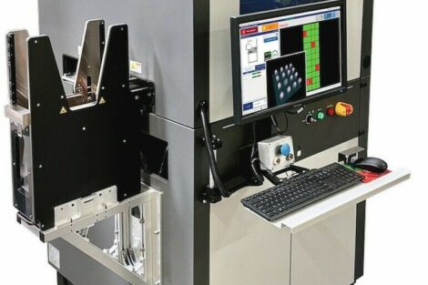
RTX inspection is often the first analytical tool used when evaluating a BGA with a potential failure or for general inspection after production. The non-destructive RTX analysis allows for the evaluation and inspection of each individual solder joint underneath the component, that otherwise would not be visible. Below are several characteristics that are evaluated during inspection with X-ray.
Real-time X-ray inspection
Bridging — an overall 2D image allows for inspection of bridging or shorting between individual solder joints.
Proper pad alignment — an overall 2D image allows for inspection of the overall alignment of the BGA solder joints with the corresponding PCB pads. Oftentimes with tin/lead (Sn/Pb) solders if the BGA is misplaced slightly off of the pads, the BGA will self-align during reflow. This is not the case when using some lead-free alloys, particularly SAC305. If the BGA is not properly placed and centred on the pads, it will not self-align on the pads. This is often caught during general inspection after production.
Voiding —can be assessed by viewing an overall 2D image of the solder joints. Some voiding is expected. Excessive voiding points to a process related issue.
Adequate ball collapse — a 3D image of the solder joints can show proper reflow of the solder balls beneath the BGA. Proper ball collapse, however, is not an indicator of the degree of wetting to the PCB pad.
Opens/Fractures — viewing the BGA solder joints in 3D also can show open connections if present and sometimes solder joint fractures, if the fracture is significant. Microfractures generally are not detectable with X-ray analysis.
The Dye and prye technique relies on the ability of a low viscosity dye to penetrate fractures while under a high vacuum. Generally vacuum is applied for several hours, followed by a high-temperature bake. This analytical technique is destructive.
Dye and pry analysis
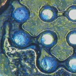
Next, the BGA is mechanically removed and the interfaces inspected for any traces of the dye on the surface of the pads. If the bonds are intact, dye will not penetrate and stain the pads. However, if there is a complete or partial fracture, the dye will coat the fractured surface and subsequent inspection will identify the open solder joints. This analytical technique is destructive. This method is used to determine if opens/fractures exist and at what interface. It also shows if the opens/fractures are concentrated to a specific part of the BGA, like a certain quadrant or if it is a random problem. Many times dye and pry analysis will be performed prior to any microsections to determine where the micro-section needs to be taken in order to have the highest probability of capturing the failure in the micro-section.
Micro-sectional analysis
Micro-sectional analysis in conjunction with scanning electron microscope (SEM) imaging with EDS capability is a very informative method for gathering both mechanical and materials information from a solder joint. Micro-sectional SEM analysis can confirm proper ball collapse as evidenced through X-ray. It also can provide information as to the degree of wetting to the PCB, and component pad and the amount of intermetallic (IMC) that was formed during reflow. Elemental data can be obtained from the bulk solder to determine composition of the alloy. A chemical etchant can be applied to the solder prior to imaging to show the grain structure of the solder. This allows for analysis of the solder itself to determine proper alloying of the metals in the solder, which relates to the amount of heat and dwell time during reflow.
All three of the methods described above are used during failure investigations and also as part of assembly construction analysis prior to full production of the assemblies. It is never a bad idea to sacrifice one or two assemblies up front for validation of the BGA attachment process prior to high-volume production. While there is some cost involved with analysis, validating a process before production is always less costly than scrapping or reworking thousands of assemblies.
EPPE 429
zusammenfassung
Die Bestückung von BGAs nimmt in der Elektronikfertigung einen immer höheren Stellenwert ein, und geht damit in eine komplett andere Welt der Inspektionsmethoden. Da die Lötstellen oftmals verdeckt und deshalb mit bloßem Auge nicht erkennbar sind, werden neue Vorgehensweisen beim Testen notwendig. Der Artikel diskutiert sämtliche Formen einer Störung beziehungsweise eines Ausfalls und stellt Werkzeuge sowie Methoden zu ihrer Vermeidung vor. Die bessere Lösung ist, einen Prozess bereits im Vorfeld zu untersuchen, statt hinterher zu reworken.
L’importance du montage des BGA dans la production électronique ne cesse de croître et ouvre ainsi des horizons totalement nouveaux en matière de méthodes d’inspection. Etant donné que les points de brasage sont fréquemment recouverts et donc invisibles à l’œil nu, de nouvelles procédures de test sont nécessaires. L’article détaille toutes les formes de défauts ou de pannes et présente des outils ainsi que des méthodes de prévention. Car la prévention constitue la meilleure solution : une analyse préalable du processus est préférable à un réusinage.
Since 1982, STI Electronics, Inc. has been the premier full service organization for training, consulting, laboratory analysis, prototyping, and small- to medium-volume PCB assembly in the electronics industry. STI also produces a complete line of solder training kits and training support products. Additionally, the company distributes products for the electronics and industrial markets.
Share:
