The continuous improvement in the scaling and integration capabilities of IC technology has led to develop 3D interconnection and packaging technologies. Stacking the functional ‘tiles’ on a chip in three dimensions can significantly reduce chip area. In addition, it can result in much shorter interconnects between the tiles, thus reducing the problems associated with interconnect delay and power consumption.
3D interconnects may be achieved at different levels of the interconnect hierarchy. They can be achieved at the chip level, interconnecting the ‘traditional’ pins of the die in the third dimension (3D SiP – system-in-package – approach). This technique is however restricted to stacking of dies with limited pin count and limited interconnectivity between the die. When much higher interconnectivity between dies in the stack is required, a 3D SoC – system-on-chip – approach is more suitable. In this case, interconnections between circuit blocks of different dies behave as on-chip ‘global-wiring’ interconnects with low resistance and capacitance, allowing for faster interconnects and/or low-power interconnectivity.
Finally, 3D interconnects are envisaged at the lowest level, i.e. the transistors themselves, where technology focuses on integrating more transistors per unit area. In this case, 3D interconnects are only local interconnects and the global on-chip interconnect layers remain essentially 2D interconnect-layers. This approach is referred to as 3D integrated-circuit or 3D IC-technology.
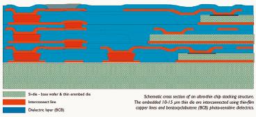
Methods need to be developed for the efficient manufacture of 3D SiP, SoC and IC systems. Imec focuses on the development of both 3D SiP-integration schemes and enabling technologies for 3D SoC-structures. An example of such a 3D SiP-integration scheme is a fully integrated low-power RF transceiver, which was previously developed. An important contribution to the 3D SoC-approach is the ultra-thin chip-stacking (UTCS) technology, currently under development. In a typical UTCS structure, ICs are thinned down to 10 to 15µm and embedded inside a multilayer thin-film build-up, realized on a base CMOS wafer. This requires very aggressive wafer and die-thinning techniques, eventually reducing the die to the active circuit layer. The use of very thin layers improves the 3D connectivity because it relaxes the required aspect ratios for these structures, and also improves the thermal performance of the stack. Besides die-thinning solutions, a technique is required to transfer the active die, thereby preserving its electrical integrity. Research at IMEC on 0.35µm CMOS test-dies before and after thinning to 45µm (wafer level), and after further thinning to 15µm and transfer to a host substrate, has shown that standard CMOS die can be thinned to very thin layers without a loss in yield. Further improvement can be obtained by combining UTCS technology with the through-wafer via technology. Using this technology, very thin-film via connections can be achieved with pad sizes smaller than 50µm, resulting in very high interconnect densities in the third dimension. This technology is subject of further development.
EPP EUROPE 439
Share:


 and 3D system-on-chip (SoC) id=)