Due to the shortage of components in the electronics industry and the dependence on Asian suppliers, the European Community has decided to double Europe’s global market share in the semiconductor industry to 20% by 2030. This requires huge investments in new production and research capacities. To achieve this goal, the EU launched the „European Chip Act“ on February 8, 2022, which will mobilize 43 billion euros in public and private investment.
At the same time, we are seeing a trend toward multi-chip packaging. Moore’s Law no longer applies. The cost of developing smaller structures is too high, but the possibilities and advantages of combining different chips and components in one package are promising. Complex functions of entire devices can be integrated into a small BGA or IC package. This trend affects all packaging processes from 2D to 3D to wafer-level packaging.
The packaging process is becoming more complex and challenging, but new interconnect methods such as hybrid bonding and interposer materials are enabling higher density and higher levels of integration. Smaller components, higher density and new materials are challenging existing inspection and measurement systems. Customized measurement equipment is needed to support the new packaging trends. Especially when the boundaries between front-end and back-end applications or back-end and SMT become blurred.
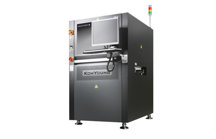
3D Moiré interferometry measurement is the latest standard in SMT. Due to the proven robustness and reliability of this measurement, these machines have been used in semiconductor packaging for several years.The online seminar shows the adaptation of the well-known Moiré interferometry principle in SemiCon and packaging applications.
More useful information to be received during a KohYoung webinar on September 15, 11:00 am. For an immediate registration please click here.


