
XSiL is a world-leading provider of innovative laser micro-machining systems for high-volume manufacturing for the semiconductor, opto-electronic and bio-medical sectors. At Semicon West the company has launched the X300D+, its new laser dicing system specifically designed to process thin silicon wafers. In an interview with EPP Europe Brian Farrell, the new CEO of XSiL, talks about this new product and about his plans.
What are the demanding requirements of thin wafer dicing?
For thin devices and stacked packages, yield is more important to chip manufacturers than ever before. Manufacturers care about cost-of-ownership (CoO) but this is under significant pressure for thin wafer dicing because of lower yield, lower throughput and rising consumable costs. As wafers are getting thinner, these issues are harder to overcome. Regarding yield, there are three main interrelated concerns: the reduction of wafer thickness, the use of Die-Attach Films (DAF), and the greater emphasis on die strength, as a die with greater strength will provide higher yield in packaged form. Costs are, of course, another major concern; they arise firstly from the required capital equipment capacity to meet the end-product device demand. Consumable cost is the other concern, including resources such as gases, water, electricity, but also costs associated with labour and opportunity costs, that is, down time.
What are the drivers for this new product?
Driven by consumer demands for memory, power devices, smart cards, etc. wafers are getting thinner; current production is at 75 µm, some at 50 µm, with roadmaps for thinner devices. The volume of thin wafer production is also increasing. Lasers offer some valuable benefits for thin silicon processing, such as high cutting speed, which increases when thickness decreases. In this growing thin wafer market, and as common dicing systems show limitations in regards to the specific requirements of thin wafers, XSiL has developed a laser-based tool that directly addresses the main industry issue – yield. Yield from the overall packaging process is vital, but more so in recent times. As packaged devices become more complex, there are more involved and evermore interrelated process steps; backgrinding to thin wafers to ever decreasing levels, stress relieving steps, de-mounting and re-mounting, thin wafer and DAF dicing, new wirebonding techniques for multi-level chips, etc. The challenge for all packaging manufacturers is attaining and sustaining high yield. One can imagine a mini-SD 4GB Flash device with multiple die in a stacked configuration; the opportunities for failure and the cost of yield loss on the entire packaged device is now far greater than that on a single die package.
With thin wafers, present singulation techniques are facing increasing difficulties. Why? Could you briefly explain to us what the present singulation techniques are and why they are facing increasing difficulties?
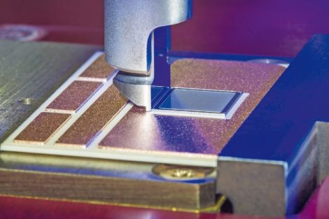
Abrasive sawing is the most common dicing process, where a diamond blade is used to mechanically saw the silicon. However, with the growth in thin wafer dicing, new issues that impact device yield and provide increased complexity for traditional dicing saws arise, due to reduced wafer thickness, use of DAF and greater emphasis on die strength. The predominant mechanical saw dicing method is today encountering cost-of-ownership issues. Yield is the largest factor, but so also is reduced throughput and rising consumable costs. Traditionally, the ratio of the bulk silicon layer to the patterned device layer has been large enough to not present undue blade dicing concerns. Now with thin wafers, this has changed significantly. It is not uncommon to have for example a 6 to 10 µm patterned layer, 75 µm of silicon and 25 µm of die-attach film. In this scenario, the mechanical impact of saw blades causes greater stresses on the wafer, resulting not only in increased chipping, cracking and delamination, but also in poorer DAF singulation and lower die strength (due to chipping and other stresses produced on the die sidewall) – ultimately lower yield. DAF present problems for traditional dicing techniques, as their use has a tendency to increase back-side silicon chipping, as well as loading the diamond tipped blades with polymer and reducing the blade life. To somewhat overcome this, more expensive dual spindle saws are required so that one blade type makes a step cut and other makes a through cut. Needless to say, there are increased consumable costs – more frequent blade changes, more DI water consumption. In addition, it is reported that dicing speeds have to be reduced significantly, to about 25 to 30 mm/s. This increase in capital cost and consumable costs with a reduction in throughput is a hard pill to swallow. To make matters worse, as wafers get ever thinner, these yield and throughput issues become more onerous. Because of increasing cost pressures, chip manufacturers are actively seeking alternate solutions to achieve higher yield with higher throughput – a better cost-of-ownership (CoO).
Where do you see the advantages of laser dicing technology?
Neither blade nor laser alone is sufficient to achieve and maintain high yields on thin wafer dicing. While the laser approach achieves high throughput and can contribute to higher yield, an additional process is required to complement laser dicing to address die strength. In the X300D+, a laser-based approach is complemented by an innovative process called MaxFlex to provide die strength enhancement after dicing. In addition to this process, the system includes coating and cleaning activities.
What are the specific strengths of the new laser-based X300 D+ system for processing wafers below 100 microns?
While this laser-based approach provides high throughput and high yield in comparison to other offerings for thin silicon dicing, it also provides low consumable cost in exchange for this level of yield. With low coating costs, minimal DI water consumption and directly attributable etch to yield costs per wafer, a more competitive CoO is attained. As wafers get thinner, there is good news for device and packaging manufacturers. Laser dicing speed increases resulting in increased throughput for the same high levels of yield. In addition, consumable costs decrease as the etch cost reduces in proportion to the area of exposed silicon after dicing. This results in an ever improving return on capital and removes some of the technical and cost barriers to widespread thin and ultra-thin wafer adoption.
Will the same product be launched in Europe? – If so, at which trade show?
All our European customers have had direct contact from XSiL, most are travelling to Semicon West. After the show, we will be visiting them all again and will also have meetings around Semicon Europe in Stuttgart.
What are your European customer’s biggest challenges and opportunities for the coming year?
Their biggest challenges are the same as they are for our Asian and US customers: Competitiveness. Cost of manufacturing devices in Europe can be higher than Asia where labour rates are the driving factor, however, increased productivity through innovation and automation can offer opportunities to allow Europe continue to be competitive.
We are hearing a great deal about Eastern Europe, is your company active there?
At present we have no sales in Eastern Europe although we have plans to target this area.
Can Europe compete with Asia?
Europe can and does compete with Asia at a certain level. It is an over simplification to consider Asia as one bloc – Taiwan, Korea, and Japan have all been successful for very different reasons. China is showing rapid expansion, again for different reasons. Europe has a core knowledge base in semiconductor manufacturing that will not go away. Many European companies will further outsource to Asia to remain competitive.
Which parts of Europe are the current star performers for XSiL? And do you see any particular reason for this?
Historically the MEMS industry has been a very successful sector for XSiL, with Europe being well represented as a portion of our sales. Europe has led the initial push in the MEMS industry.
You have recently been appointed to the position of company CEO. Could you give us a short overview of your background and about your plans for the company?
I am a co-founder of XSiL and have served as the company’s Vice President of Engineering since its foundation in April 2000. I was appointed CEO in June 2007, replacing Peter Conlon. Prior to XSiL, I was a founder of MV Technology, where I served as Vice President of Engineering until it was sold to Agilent Technologies. I completed an BA in Mathematics in 1987 and an BAI in Mechanical Engineering in 1990, both at Trinity College Dublin. I then completed a Masters in Engineering Design (MED) at University College Dublin in 1996. Our plans are to position XSiL to take advantage of the rapidly expanding laser dicing market. The management team are preparing XSiL to leverage from its existing technology base in laser machining and via drilling to open new application areas in dicing and scribing for semiconductor manufacturing.
Your Company has recently moved into your new facilities in Dublin. What are your plans for the European operation, will there be many changes?
Plans are to retain R&D in Europe at our new facilities. In June 2007, the company headquarters were relocated to satisfy the need for bigger, more modern facilities. We will continue to expand other functions of the company into the regions for system sales growth (mainly in Asia). Currently, we have subsidiaries, sales representative and technical support and subsidiaries in the US, in Japan, in Taiwan, in Singapore and in Korea.
EPP Europe 406
Share:


