In the medium term, only those electronics producers that meet the highest quality requirements and optimize their production processes will stay in business. To avoid defects, the causes must be identified and systematically eliminated. Linking various inspection gates creates wide-ranging possibilities for cost optimization and process reliability and permanent improvements in product quality. Constant development of inspection technology is essential.
Without doubt, the electronic design of a product must primarily meet customers’ expectations. But developers should also take into account costs for material, production and inspectability and adapt their concept to these requirements. In this way, later production errors and unnecessary costs can be avoided. E-CAD designers in a company with its own production can take advantage of the short communication paths and discuss necessary production processes with the in-house experts. Companies that rely on the support of an EMS service provider (electronics manufacturing services) for manufacturing should contact the specialists working there. Performance of failure mode effects analyses, abbreviated FMEAs, is recommended. With aids such as the Ishikawa diagram, developers and experts can together determine what influence the 5-Ms (manpower, machines, methods, material, measurement) and the related risks have for the origination process of the product. The goal is to produce innovative products with no defects in an optimized production process.
Data from experience are important for evaluating risks correctly. In electronics production, automatic inspection systems provide such experience continuously in the form of both data and images. Results from solder paste inspection provide information about the quality of the solder paste print designs and of the printing process. The print template used is created based on Gerber data generated from the E-CAD system. If the specifications defined in it are not optimally adapted to the production conditions, there will be systematic solder problems. The aperture geometries of solder paste surfaces in the E-CAD system should be coordinated regularly between the developer and the production expert responsible for the solder paste print. The SPI system (solder paste inspection) provides the data required for efficient coordination.
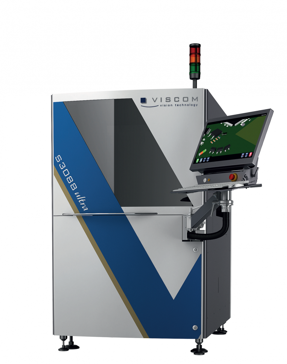
The Viscom solder paste inspection system, for example, has interfaces with both the paste printer and the assembler. In accordance with Industry 4.0, the result data from the downstream SPI system is read by the printer and correction measures are automatically introduced, such as template cleaning or correction of a template offset. With increasing miniaturization, transmission of the SPI result logs to the assembly machines is becoming more and more important, as assembly of very small components (01005, 03015) and of components with small pitch (< 500 μm) to the actual position of the solder paste has been shown to result in fewer defects than assembly of the components to the target position relative to the register mark in the copper.
In addition, the results of the solder paste and assembly inspection before the oven can be clearly merged with those of the post-reflow solder joint inspection with AOI and X-ray. The data and images gained can be used by both the process owners and the product developers to identify and systematically eliminate causes of defects in the process and design. Special software tools, such as the Viscom Quality Uplink with Viscom Uplink Process Analyzer (VUPA) or the Viscom SPC software (statistical process control) help with evaluation and visualization of the many results collected by Viscom inspection systems. The advantages include a reliable separation of classes between genuine defects and false calls (false reports). Many possibilities are thus available to take process-relevant information into account early and thus optimize the production process. This is especially successful when reaction times can be kept as short as possible. To achieve this, Viscom offers the possibility to have all process-relevant data available on smartphones and tablets.
About the presentation
Electronics designers rely on data from experience for their development work. Automatic inspection systems not only reliably detect defects, but also provide important quality data and microscopic images of defective layouts. This is an important contribution to future avoidance of design-related defect causes. In the production process, in turn, costs are optimized, process reliability is increased, and product quality is improved through linking of the data of different inspection gates.
Benefit statement
Electronics manufacturers must constantly optimize their production processes using the latest inspection technology. Development of an attractive, easy to produce, but still robust product today requires close interaction between all who participate in the origination process. Intelligent inspection significantly helps to optimize solutions, processes and costs, from development to production.
Listen to the presentation live at
 Budapest, May 25th, 9am – 5pm
Register for FREE
Please use the registration code OLHUN17.
