Consumers are demanding ever more powerful, lightweight and compact electronic devices. Handy and compact products and solutions are therefore in high demand, and competition between suppliers is fierce. Manufacturing technologies and miniature components that enable such mobile devices to be continuously reduced in size and weight have moved sharply into the focus of designers and manufacturers alike. The use of cavities (trenches) in electronic assemblies is another efficient method of creating even more compact electronic circuits, opened up by the use of the third dimension (cavity) in packaging.
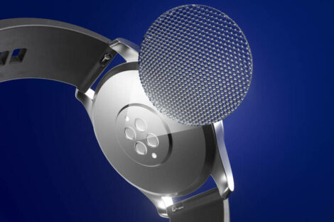
The user demand for increasingly thinner and lighter, and powerful electronic devices such as wearables or cell phones has led to a new kind of complexity in packaging density. Generally, a finished product consists of several components such as display, battery, camera, sensors, mainboard and so on. When it comes to the camera in a cell phone, for instance, the size and shape are characterized by the lens configuration; display size is dictated by the application; batteries meanwhile are more likely to increase rather than decrease in size and capacity because the engineering goal is to attain maximum achievable operating times. This means that considerable savings in weight and size for mobile devices can only be achieved through changes to the circuit board or electronics assembly. One way of reducing the important influential elements, and which has not been widely used up to now, is the placement and soldering of components in cavities of the circuit – something that can be achieved relatively easily.
The potential for reducing dimensions in this way is not exclusive to devices but also applies to single components. Placing an LED in a cavity on an IC leadframe, for example, significantly reduces the height of the component. In addition, with the subsequent application of encapsulation material, one can better protect this LED against environmental influences and increase the service life of the electronics.
To ensure that this ‘third dimension’ manufacturing process can be used efficiently, and even at high production volumes, the proven method of stencil printing solder paste is the ideal option. This is because this process is well established in the industry, is fast and inexpensive, and users have a high level of experience with this procedure. In addition, excellent equipment is available, cycle times are very short and the repeatability of the individual steps is high.
The biggest challenge of applying solder paste to cavities in electronic assembly is having to operate simultaneously on different levels of the object. When providing solder paste to the top of the leadframe and simultaneously to the bottom of the cavity, for example, the squeegee must work extremely evenly and precisely.
Creating the test setup
With a high level of expertise in the area, the Christian Koenen Application Center supports the technological development of both assembly technology and manufacturing processes in electronics. In this way, the Center performs a key function, ensuring that the best possible solutions for complex requirements can be developed at a high level of efficiency, and in collaboration with industrial clients.
Together, the companies Heraeus, Koh Young, EKRA, and Christian Koenen, developed an optimal test setup for the reliable printing of LEDs in cavities. The verification steps required were carried out under real production conditions. In the manufacturing process that was simulated, off-the-shelf components and materials available on the market were used.
The systems and materials used in the test and verification process were:
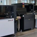
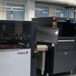
- ASYS SMT line, consisting of EKRA SERIO 5000 printing system together with various transport and handling modules.
- Solder paste LED131 SAC type 6
- CK 3D-stepped stencil and slit squeegees
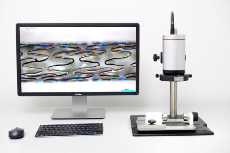
- Koh Young inspection system Meister S (SPI)
During the test series, several leadframes were printed with solder paste. The bottom side cleaning in the printer was disabled because the impact of the cleaning here was not to be assessed. A special slit squeegee was used for printing, with the individual segments of the squeegee sliding in and out of the cavities during the printing process. For this purpose, both squeegees for the different print directions had to be precisely aligned with the cavities. The highly precise iQUESS squeegee holder and the stencil unit with alignment assistance optimized for this application were the essential pieces of equipment needed here. We checked the prints immediately afterward in the Meister S inspection system. To further verify the results in the test series, we also used various microscopes and a Cyber laser scanner. The printed leadframes were, however, neither assembled nor soldered afterwards.
Selection of solder powder and paste formulation
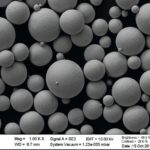
For the process of applying solder pastes into the cavities of the LEDs, very fine solder powders with small grain sizes of 15 µm were required for use with 3D-stepped stencils. Such solder powders significantly reduce potential printing errors such as fluctuating solder volumes or solder paste depots that are not completely filled. For the study described here, the special SAC305 Type 6 solder powder, manufactured using the patented Welco technique, was used. In the production procedure, the solder alloy is first heated in a temperature-stable dispersion medium above its melting range. A special rotor-stator process is employed to produce molten, homogeneous solder particles. This ensures that, after cooling, the required fine solder powder fraction has a very narrow particle size distribution (Type 6: 5–15 µm). It is characterized by very good sphericity (aspect ratio of ~1) and a smooth surface of the spherical shape. These solder powder properties help to ensure both very good initial printability as well as the required stability in long-term printing. These criteria will be of particular importance when it comes to ramping-up 3D-stepped stencil technology in manufacturing.
In order to secure, not only excellent printability, but also the necessary good solderability with this ultra-fine solder paste, Heraeus has developed the LED131 NC flux series which has been tailored for use in printing in cavities, and with which the high wetting requirements can be met. Due to the smaller grain size, the surface area of the solder powder spheres increases considerably (high oxidation susceptibility), so for the necessary activation, a robust formulation had to be developed first. The aim was to achieve good wettability of all the joining surfaces involved (especially those of components and substrates) and a minimal void rate, while at the same time maintaining the necessary high surface isolation resistance (SIR) of the remaining flux residues. In addition to these considerations, as well as other standard requirements for solder pastes such as low slump and a low tendency to form solder balls, it was necessary to guarantee that the solder pastes had the appropriate tackiness. This ensures that the solder paste can be easily removed from the stencil and that its adhesion to the leadframe surface is ensured.
Printing stencil technology
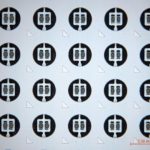
One of the biggest challenges in the design of the stencil is the peculiar shape of the leadframe. The cavities on the leadframe are not angular, but circula meaning the use of a classic slit squeegee is not possible. Leadframes for use with LEDs, displaying the positions of the solder deposits, are shown in the illustration (see page 26, bottom right).
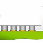
3D step stencils are used for printing in cavities. These are made using the Koenen company’s patented process. In this procedure, the base material of the stencil is removed layer by layer on both sides with the highest precision. As shown in the diagram (see page 27, top right), the stepped stencil with the substrate is displayed in cross-section.
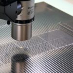
Following this production step, the apertures are lasered into the cavity and afterwards chamfered in the cavity using a very specific process. The printing area of the 3D step stencils including the apertures is shown in the image (page 28, bottom right).
The slit squeegee used, just like the stencil, was designed to be equipped with special markings. These allow for the precise alignment of the squeegee to the stencil. If, for example, the squeegee slots are not aligned with the cavities in the printing direction, the squeegee cannot slide into the cavities and the dots will not be printed.
Printer featuring advanced print head
We printed the paste in the test series using a printing system from the scalable SERIO platform. This modern printer range can be retrofitted with all the relevant functions required for the evaluation conducted. Stencil printing reaches its full potential when applying paste in cavities. Very high throughput rates can be achieved through an industrialized and easily controllable manufacturing process with high yields.
The characteristic height differences of stepped stencils require specific procedures in the printing process, and, for efficient printing, the equipment also needs to display some special technical features. If the paste transfer is realized via slotted squeegee blades, the positioning and alignment of the blade sections relative to the layout and squeegee stroke are crucial. This ensures the uniformity of the paste application across the substrate.
The stencil and squeegee unit in the SERIO printer are in a fixed position relative to one another. This means that the best possible position for the stencil is precisely set at the start and will remain accurate over the complete production run, and again and again. A high-precision, camera-based set-up for the stencils is of great importance here. In addition, screws on the bars of the stencil support and the squeegee holder can also be altered if required. This way, the position of the squeegee can be precisely adjusted transverse to the printing direction – absolutely matching the topography of the stencil.
The optimum orientation ensuring the machine parts and the stencil are in exact relation to one another also has the advantage of making the peeling process on the stencil top of the Advanced Print Head as gentle as possible, significantly reducing wear. The squeegee blade peeling process takes place on two different surfaces: one on the top of the stencil and one on the deeper surface within the cavity. It must be ensured that the squeegee is printing with continuous force across the entire blade stroke. The pneumatically controlled EKRA squeegee head with closed-loop control guarantees this by permanently comparing the target and current values of the pressure force. In the present version of the Advanced Print Head, an even narrower tolerance window has been achieved. If the stencil steps and cavities are asymmetrically distributed over the print area, the oscillating movement of the squeegee can be limited through adjustment screws to improve the peel-off behavior.
3D measurements and pixel heights
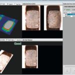
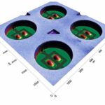
All 3D measurements (of the paste application) were based on heights information acquired using the inspection system Meister S. The height information from each single camera pixel combines to provide a three-dimensional topography of the measured object. By using position, gray value, and height filter, the pixels which represent the height values of the printed paste volume can be determined. This is then made up of the sum of the pixel heights multiplied by the pixel area. It follows, then, that the smaller the pixels, the more precise the volume calculation.
Pixel heights are determined using relative measurements of the area around them. For usual system applications such as those on printed circuit boards and ceramic substrates, this method is the correct and reasonable approach. When we print into a cavity, however, how does this work? In such an application, determining the zero line needed for the measurement of the relative height becomes difficult. Additionally, the user is confronted with a lot of measurement noise due to the influences of the surrounding area such as the high rim of the cavity. So how can we overcome these measurement challenges?
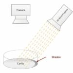
If there is not enough space in the cavity, the inspection algorithm calculates the reference height outside the cavity and measures the height in a negative direction. The result is thus inverted. If the space is sufficient to determine the reference height, however, then the walls of the cavity will still distort the measurement. Due to the higher outer surfaces, an interfering signal can occur, since the reference height is probably outside the regular measuring range. Moreover, there is a disturbing shadow effect. This is because the projected moiré pattern (the measuring light) is partially blocked by the edges of the cavity.
The Meister S inspection system has been designed to overcome this challenging measurement issue and therefore delivers excellent results. Special filters, known as ‘jig noise filters’, eliminate the measurement noise caused by the edges of the cavity. These filters are also used for the measurement of small substrates in a workpiece carrier. The inspection system uses various pieces of information to determine the reference height. If there is not enough space in the cavity, the heights of local and global alignment marks are used, or freely definable reference points can be set. The Meister S uses four 3D projector units to generate the moiré information. By superimposing the information from all four projection modules, shadows can be fully eliminated because the cavity is completely illuminated from all four directions. Last but not least, the small pixel size of 5 µm guarantees a very precise 3D reconstruction of the printed paste, thus ensuring a high repeatability of measurements with a Cgk 10%.
A continuing partnership
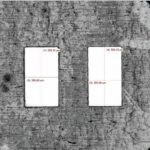
By combining solder paste, stencil, printer, and SPI system, the partnering companies successfully developed and verified an efficient method of solder paste printing in the cavities of LED leadframes. This suggests that electronics manufacturers on an industrial scale will be able to replace a formerly time-consuming and expensive dispensing process with a proven, cost-effective, and reliable stencil printing process. This will enable both an increase in throughput rates and an improved repeatability of the process steps. As the graphic documentation of our investigation shows, leadframes were able to be printed successfully and efficiently.
The partners in this project will continue to develop research and technology in this direction, in order to ensure that the results of this investigation, as well as others, can be utilized for other manufacturing tasks. In general, the team‘s goal is to find efficient, technically sophisticated, and affordable solutions using their combined expertise. Throughout this cooperation, we will continue to pick up on new trends and production technologies and will be putting the feasibility of solutions to the test in a practice-oriented manner. This, and the individual expertise of each company in the partnership, helps facilitate the ‘out-of-the-box’ thinking necessary to create a winning team.
Zusammenfassung Résumé Резюме
L‘impression dans les creux des grilles de connexion des LED (leadframes) avec de la pâte à braser a été développée et testée avec succès en partenariat, dans le cadre d‘une coopération. Les fabricants d‘électronique peuvent ainsi remplacer le processus de dépose par l‘impression au pochoir, ce qui permet d‘augmenter les débits de transfert et d‘améliorer la reproductibilité de l‘étape du processus.
L‘impression dans les creux des grilles de connexion des LED (leadframes) avec de la pâte à braser a été développée et testée avec succès en partenariat, dans le cadre d‘une coopération. Les fabricants d‘électronique peuvent ainsi remplacer le processus de dépose par l‘impression au pochoir, ce qui permet d‘augmenter les débits de transfert et d‘améliorer la reproductibilité de l‘étape du processus.
L‘impression dans les creux des grilles de connexion des LED (leadframes) avec de la pâte à braser a été développée et testée avec succès en partenariat, dans le cadre d‘une coopération. Les fabricants d‘électronique peuvent ainsi remplacer le processus de dépose par l‘impression au pochoir, ce qui permet d‘augmenter les débits de transfert et d‘améliorer la reproductibilité de l‘étape du processus.
L‘impression dans les creux des grilles de connexion des LED (leadframes) avec de la pâte à braser a été développée et testée avec succès en partenariat, dans le cadre d‘une coopération. Les fabricants d‘électronique peuvent ainsi remplacer le processus de dépose par l‘impression au pochoir, ce qui permet d‘augmenter les débits de transfert et d‘améliorer la reproductibilité de l‘étape du processus.
L‘impression dans les creux des grilles de connexion des LED (leadframes) avec de la pâte à braser a été développée et testée avec succès en partenariat, dans le cadre d‘une coopération. Les fabricants d‘électronique peuvent ainsi remplacer le processus de dépose par l‘impression au pochoir, ce qui permet d‘augmenter les débits de transfert et d‘améliorer la reproductibilité de l‘étape du processus.
L‘impression dans les creux des grilles de connexion des LED (leadframes) avec de la pâte à braser a été développée et testée avec succès en partenariat, dans le cadre d‘une coopération. Les fabricants d‘électronique peuvent ainsi remplacer le processus de dépose par l‘impression au pochoir, ce qui permet d‘augmenter les débits de transfert et d‘améliorer la reproductibilité de l‘étape du processus.
L‘impression dans les creux des grilles de connexion des LED (leadframes) avec de la pâte à braser a été développée et testée avec succès en partenariat, dans le cadre d‘une coopération. Les fabricants d‘électronique peuvent ainsi remplacer le processus de dépose par l‘impression au pochoir, ce qui permet d‘augmenter les débits de transfert et d‘améliorer la reproductibilité de l‘étape du processus.
L‘impression dans les creux des grilles de connexion des LED (leadframes) avec de la pâte à braser a été développée et testée avec succès en partenariat, dans le cadre d‘une coopération. Les fabricants d‘électronique peuvent ainsi remplacer le processus de dépose par l‘impression au pochoir, ce qui permet d‘augmenter les débits de transfert et d‘améliorer la reproductibilité de l‘étape du processus.
Печать паяльной пастой в углублениях выводных рамок светодиодов может быть успешно разработана и протестирована в рамках партнерского сотрудничества. Таким образом, производители электроники могут заменить процесс дозирования трафаретной печатью, что повышает производительность и улучшает воспроизводимость технологического процесса.
