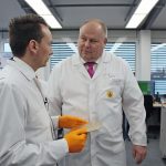
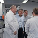
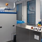
A live demonstration of the application center was one of the main highlights of this day. The team for the application center, Sebastian Bechmann and Daniel Rudolph, took the visitors around the center, with the help of representatives from partners, including Ekra, Asys, Koh Young, Ersa, Wagenbrett, kolb Cleaning Technology, and GMS. Opened since 2008, it was built and configured with the customer in mind. A variety of services are offered, to analyze and test theories, before bringing the results to a real production. Customers can take advantage of the resources it includes, target it to the needs of their specific processes in order to find optimal solutions, reduce costs, and increase quality. The team also assists customers with measurement of PCBs, pad and opening sizes, as well as, 3D measurement of deposits, and more.
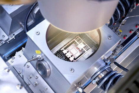
The center includes an X5 STS screen printer from Ekra, a PB46 printing and balling machine from Wagenbrett, as well as a stencil printing and rework system Hybrid Rework 550 (S1) from Ersa. As part of the inline concept, a Series 5000 printer from Ekra, a SPI system 8030–2 from Koh Young, and a board handling system from Asys can be found. On the same floor, a cleaning area is also part of this application center. For cleaning screens, stencils, and substrates, it is equipped with two fully automatic cleaning systems, a PS 300 from kolb Cleaning Technology and a MC4000 from GMS. Manual cleaners are also part of this area which supports smaller cleaning processes.
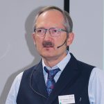
Dr. Thomas Ahrens, Trainalytics GmbH
DoE (Design of Experiment) as tool for paste printing optimization
The goal is to always have an optimal manufacturing in an SMD assembly, establishing reliable solder joints. Especially with paste printing, it may become complex to find what works best, as there are a variety of different processes, techniques, trends, and materials that can be used. This is why a plan needs to be put in place to achieve these optimal steps towards productivity. In order to do this, testing needs to be done to find what works best. According to Dr. Thomas Ahrens, there are different ways to achieve this, which include different experimental tests. Trial and error or the best guess are methods frequently used can be methods used, although these may not be very accurate. Instead, he suggests to use Design of Experiment (DoE) techniques, which is the act of gathering as much information as possible based on influencing factors, to evaluate an experiment.
The specific approach used will depend on the goal of the experimental design and the desired end results. For instance, which processes should be optimized, how big of an optimization is it, as well as, how much effort should be made into it should first be considered. By using the fully partial factorial design, will track all available combinations and bring more conclusive results, but this also increases the effort put in. However, the partial factorial design is best used for more complex experiments, as it reduces the scope to the strongest combinations, however it is not the most accurate. By using DoE, all parameters and combinations can be tested to find the best process to be used for an assembly, and everything is recorded for future use.
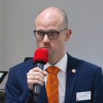
Christoph Hippin, Endress+Hauser SE+Co KG
Stencil printing challenges for SOT and SOD components
In recent years, miniaturization has been a prominent trend, and now consequences are starting to come about. There has been a higher demand for compact circuit boards and a more complex layout design, which has increased the requirements of stencil printing technology, especially when processing SOD and SOT designs. According to Christoph Hippin, this also affects the components, circuit board, layout, stencil, reliability, and rework. Ramifications can occur if these requirements are over looked, including locking gap, tilting, and twisting of the component. In order to have a reliable release of the solder paste from the stencil to the pad sizes, he believes that the openings should be 1:1. With this, due to the stencil opening being larger than the area of the top of the pad, a smaller adhesive is needed. The speaker also further discussed the benefits of using a brushing process versus electropolishing. It doesn’t create larger apertures, improves process stability, removes the least amount of material, keeps consistent thickness, and has lower edge rounding. Coating is also an important topic for stencil printing, as it reduces underside contamination and increases repeatability. Many benefits come with using the CK Plasma 3.0, including a longer stencil life with better process reliability and a better cleaning performance. Using the brushing process with the Plasma 3.0, creates a better filling, especially when it comes to miniaturization.
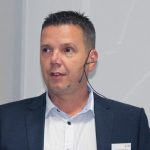
Karsten Dierker, Tonfunk GmbH Ermsleben
From prototyping to mass production- When the component mix ranges from 0402 to THR components
The speaker first went through the company’s process. Starting with defining the template parameters, to adjusting the design of the stencil, applying adhesives dots to components, then describing the adhesive application, to its final step of reflow soldering and adhesive curing. The variety of the components that the company uses were then discussed, which in turn explained why a step template from Christian Koenen was chosen. Once in use, advantages were seen especially when using the plasma coating for a secure printing process. Mr. Dierker gave specific examples of different components that needed stencil design adjustments to ensure high quality results and consequences that occurred prior to the change. These components included TSSOP 20, DFN 8, and X2SON. The reason for why 0402 and 0603 components need further adhesive dots and its benefits were also presented. The speaker then explained the different technologies used for their adhesive application, which included the DEK Stinger, which is ideal for partial fixation but not suitable for 0603 and 0402 adhesive dots. The stainless-steel screen printer is used for manual bonding and has no repeatability capabilities. For reflow soldering and SMT adhesive curing, the ASM Glue Feeder is used with Koki‘s adhesive. This flexible machine forms small adhesive dots, suitable for 0603 and 0402 components, as well as, aids in centering components during processes.
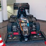
Lukas Wüsteney, Trajectory Planning db018, TUfast Racing Team
Autonomous driving- New challenges in cyber physical systems
Autonomous vehicles are no longer a thought for the future, as with the progression of technology, it is now available today. A driverless automobile does not only put the vehicle in motion, it also includes planning the best trajectory, checking for motion control, collision control, and so much more. The team of TUfast e.V. built their first racecar in 2004, and has been competing in the worldwide Formula Student competition. This competition is judged based on different categories, including specific dynamics: acceleration, handling (Skidpad), endurance, efficiency, and speed (autoX). It is also tested on statics, such as the business plan and its cost report. The engineering design is also evaluated, based on its skills, overall concept, and project management. Last year’s main focus of the competition and the racing team’s aspirations, was to build an autonomous car. With the help of Christian Koenen, they were able to make their dreams come true, with the db2018. The company sponsored this team with stencils for various electronics in the racecar, including emergency breaks, systems, and much more. With their help, they were also able to upgrade their racecar for this year, which included additional cameras, improved brake system, optimized aerodynamics, etc. They came first place in the last competition, with the hopes of winning the next one as well.
