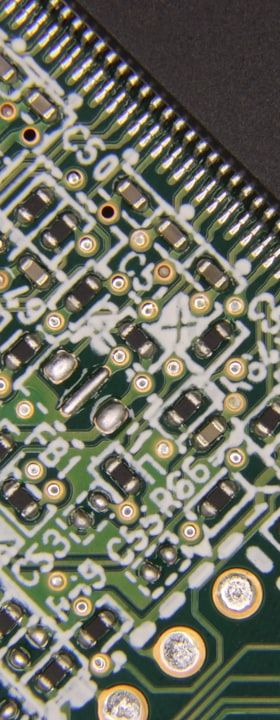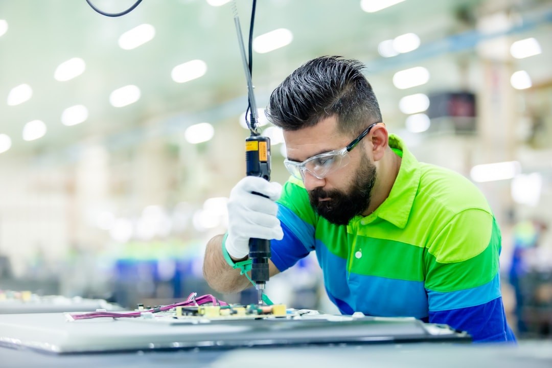
Modern printed circuit board assemblies rarely consist of surface-mount components alone. Through-hole connectors, press-fit terminals, electrolytic capacitors and power components continue to dominate specific functional segments of even highly integrated designs. For these components, selective soldering has established itself as the method of choice wherever wave soldering would compromise neighbouring SMD placements or where the thermal mass distribution of the board makes a uniform wave process impractical. The technology has matured considerably over the past two decades, yet its underlying principles and process variables remain a subject of frequent misunderstanding on the shop floor.
Unlike reflow soldering — which processes an entire board surface simultaneously inside a convection oven — or wave soldering — which exposes the full underside of a carrier to a continuous solder wave — selective soldering acts on defined, discrete areas of the board. This local action is both its chief advantage and the source of its specific process complexity.
Three Equipment Architectures and Their Trade-offs
Commercial selective soldering systems are built around three principal machine architectures: laser-driven point sources, miniature fixed nozzles and dip/drag nozzle systems. Laser-based systems apply focused infrared energy to the joint area while solder wire is fed from above; throughput is limited but the process is exceptionally clean and requires no flux management beyond the joint itself. These systems are used predominantly for repair and low-volume specialist applications.
The dominant architecture in volume production is the programmable single-nozzle or multi-nozzle system. A miniature solder fountain — typically between 4 mm and 12 mm in diameter — pumps molten solder upward through a ceramic or titanium nozzle tip. The PCB, mounted on an x-y gantry, is moved over the nozzle according to a programmed path. Alternatively, the nozzle assembly moves beneath a stationary board. Dwell time, nozzle immersion depth and traverse speed are the primary process parameters. Multi-nozzle systems operate several fountains in parallel, dramatically increasing throughput at the cost of reduced individual programmability.
A third variant, the drag soldering approach, draws the nozzle along a row of through-hole pins in a single continuous motion, approximating a localised wave. It is particularly effective for connector strips and pin headers where joint pitch and geometry are uniform.
Flux Application: The Decisive Pre-Process Step
Selective soldering is invariably preceded by selective flux application. Flux activates the metal surfaces, removes oxide layers and promotes wetting, but it must be applied only where soldering will occur — excess flux on SMD components or under no-clean areas causes ionic contamination, leakage currents and adhesion failures for conformal coating. Three flux delivery methods are standard: drop-jet fluxers (analogous to inkjet printing, offering the highest spatial resolution), mini-wave fluxers (a small flux fountain swept across defined areas) and spray fluxers with mechanical masking.
Flux chemistry selection must align with the subsequent cleaning strategy — or the absence of one. No-clean fluxes based on weak organic acids leave minimal residue that is typically benign under standard operating conditions, whereas water-soluble fluxes offer superior activation at the cost of mandatory aqueous cleaning. The quantity of flux deposited per pad is critical: too little results in dewetting and cold joints; too much leaves residue bridges and can cause solder balling beneath the board.
Thermal Management: Preheating and Solder Temperature
Through-hole components exhibit thermal masses that vary by orders of magnitude — a fine-pitch connector pin presents almost no thermal load, while a D-Sub shell or chassis ground lug can absorb several joules before reaching soldering temperature. Insufficient preheat causes thermal shock to ceramic components, activates flux prematurely or leads to incomplete hole fill as solder solidifies before reaching the far side of the barrel. Overpreheat degrades the flux and can trigger solder bridging.
Selective soldering systems typically offer top-side IR preheating panels and, in more capable machines, bottom-side convection or IR modules. A board entering the soldering station should ideally reach 90 °C to 130 °C (depending on board thickness and component population) before nozzle contact. Solder pot temperature for SAC305 alloys is typically set between 260 °C and 270 °C. Dwell time at each pad position ranges from 3 seconds to 8 seconds for standard through-hole geometries, extended for high-thermal-mass terminations.
Nitrogen Atmosphere and Solder Alloy Considerations
Selective soldering nozzles operate in open air unless the system encloses the soldering zone in a nitrogen curtain or chamber. Nitrogen inerting reduces oxide formation on the solder surface and in the nozzle pot, extends solder alloy life, improves wetting and reduces dross generation. The economics of nitrogen consumption must be weighed against joint quality requirements; for lead-free alloys — which are inherently less forgiving than tin-lead regarding wetting and dross — nitrogen inerting is generally recommended.
Alloy contamination is a specific concern in selective soldering pots. As boards pass over the nozzle, dissolved copper from pad surfaces accumulates in the alloy. Above approximately 0.3 % copper content (mass fraction) in SAC alloys, viscosity increases and wetting behaviour changes measurably. Regular alloy analysis and pot replenishment schedules are necessary to maintain process stability. Some operators use low-silver or silver-free alloys such as SN100C or SAC0307 in the selective solder pot to reduce raw material costs while retaining adequate joint reliability.
Process Qualification, Joint Inspection and Practical Integration
Selective soldering processes are qualified to IPC-A-610 acceptance criteria, which define requirements for through-hole solder fill (minimum 75 % vertical fill for Class 2 assemblies, 100 % preferred for Class 3), fillet geometry, pin protrusion and surface appearance. Automated optical inspection is generally insufficient for through-hole barrel fill verification; X-ray inspection or 2D/3D AXI systems are required to confirm fill percentage non-destructively. Cross-section analysis remains the reference method during process qualification and periodic audits.
Integrating selective soldering into an SMT line requires careful workflow planning. The process sits after reflow and SMD adhesive curing, and before final board-level cleaning or conformal coating. Board carriers or pallets are often necessary to protect bottom-side SMD components during selective soldering; pallet material (typically aluminium or PEEK-based composites) must withstand repeated thermal cycling without warping. Programming and offline simulation software, offered by most equipment vendors, allows process engineers to generate nozzle paths, calculate dwell times and predict shadowing effects before committing to first-article production.
As board complexity increases and component packages evolve, selective soldering continues to prove its value as a precision, repeatable and fully automatable alternative to hand soldering for through-hole joints in mixed-technology assemblies. Mastery of the process fundamentals — flux chemistry, thermal profiling, alloy management and nozzle dynamics — remains the foundation of consistent joint quality and long-term process capability.