3D vision inspection of packages is certainly a critical part of the backend area in semiconductor manufacturing. Here, it provides an approach for driving cost reduction and to achieve higher product quality. Fast moiré interferometry is Solvision’s technology that was recently introduced to address the issues of this inspection task.
Ronny Theriault, Solvision, Inc.
The acronym FMI stands for fast moiré interferometry. This technology was recently introduced by Solvision (European representative EPP GmbH) to address the growing needs for 3D inspection. This next-generation technology is inspired by all the advantages of moiré interferometry and other techniques. Height, coplanarity and other parameters are day-to-day challenges of 3D inspection in device packaging. This is where the FMI technology performs verification specifically for BGA, CGA, QFP, CSP and TSOP, whether they are based on ceramic or plastic substrates.
Using only one camera combined with a projector diffusing a white light pattern on the parts verified, this camera will extract simultaneously a 3D and 2D image, providing 3D heights measurements of the entire field of view, whatever area is underneath, without any scanning requirements. By using only one camera, the calibration process and maintenance of the system is largely simplified compared to technologies that require more cameras or scanning instruments.
Odd-shaped components not a problem
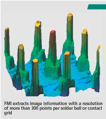
FMI differs from other methods in the inspection of BGA, CGA, QFP, CSP, TSOP and ceramics substrates since it can be used for odd-shaped packages such as PGA or CGA, and, for example, extracts information with a resolution of more than 300 points per solder ball or grid array to obtain results in the lower micron area. Since the FMI inspection technology is scalable, it can work under a very large field of view. As a result, many parts can be inspected simultaneously. This allows very high throughput, and the inspection can also verify parameters such as warpage of substrates, chip-out, peel-off and grid-to-fiducial offset (reference mark to grid offset).
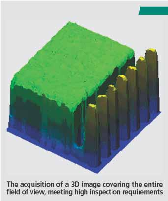
Miniaturization, speed, quality and accuracy are buzzwords in electronics manufacturing. The acquisition of a 3D image covering the entire field of view, attaining high throughputs (over 60,000 TSOPs/ hour), automated and simplified cali-bration requirements, and the easy adaptability to the next component generation are only some of the key elements that will make the difference in meeting high inspection requirements. Moreover, flexibility and adaptability are essential to meet production line installations and space contingencies. Since FMI requires very few hardware components and is simple to calibrate, integrating this technology in handlers by using an OEM kit is the easiest solution for handling and inspection. Assembly and test has to support a broad range of various packages in a very short time-to-market, hence the importance of assuring that a verification tool is flexible and adaptable to quick component, and lot changeover is also very high. FMI is a scalable technology, capable of inspecting both smaller and larger or thicker packages, and characteristics of all kinds such as PSGA, stacked multi-chip or wafer bumps and even more.
Traditional trade-offs
Traditional technologies are available on the market of course, meeting inspection requirements such as laser-based method, stereovision, etc. A laser-based approach is the point triangulation technology that provides a single-point light moving as fast as possible across an object in order to provide a height profile. When extended to high-speed area profiling, sensitive mechanisms are employed to quickly move that point around the inspected area. Spinning mirrors, polygons and precision drives are essential parts of the inspection mechanism.
Resolution in the range of 2 to 8 micron is a particular challenge for laser-based solutions, since lasers suffer from the speckle effect. Therefore, it is only sufficient for full-size ball-grid arrays but not appropriate for smaller CSPs, flip chips, etc. Though the alignment is a particular and delicate action of laser-based technology, a precise alignment of the beam is required when scanning in tray. For example, all parts have to be justified in the same corner of their pockets to assure precise alignment of the components and the laser beam. Moreover, laser technology requires two different systems for 2D and 3D inspection, since lasers do not allow for both 2D/3D inspections simultaneously.
Another technology traditionally used for inspecting components such as BGA, CSP, etc. is stereovision. It consists of using two cameras configured at a specific angle and pointing at an exact location, which leads to a rigorous calibration process between the two cameras. The stereovision technique can adjust from small to large parts, but the technique cannot provide dense data and handle free-form surfaces well (flat surfaces with no edges for references). It must also determine the shape of a component prior to the inspection process.
The fact that one of the two cameras has to be tightly held at a defined angle remarkably limits the inspection area and leads to problems in getting a clear image of the entire part. Camera auto-calibration is therefore also an issue with this calibration technique, because of the need to secure the presence of the calibration pattern in the field of view of the camera.
An outlook
High flexibility, effortless maintenance, cost reduction by combining handling and inspection, avoiding waste and rework to a great extent, better quality control and real-time process monitoring, inspection directly after solder ball reflow, all are features that describe the ability of the FMI approach and its inherent cost of ownership. Fast moiré inspection is currently the only technology performing in-process, that means verifying IC packages directly after solder ball reflow. By being connected to a production line, a direct control allows the manufacturing to be stopped when an unwanted process drift occurs. Preventive actions can also be accomplished, which can save aconsiderable amount of time and money. Since the trend towards smaller advanced packages leads to an emergence of many different types such as PSGA, stacked MCMs, leadless devices, etc., FMI provides users with presently the most flexible and upgradeable 2D/3D inspection approach.
ZUSAMMENFASSUNG
Im Backend der Halbleiterfertigung kommt der Inspektion einer hohen Package-Vielfalt große Bedeutung zu, insbesondere weil Field-Array-Bauformen und andere komplexe ICs ständig zunehmen. Aufgrund ihrer weiter reduzierten Abmessungen ist nötig, mit hoher Bildauflösung zu arbeiten und dabei dennoch großen Durchsatz zu erreichen. Nach Anbieteraussagen offeriert die Fast-Moiré-Interferometrie hier die optimale Technik.
RÉSUMÉ
L’inspection d’un grand nombre de conditionnements différents joue un rôle très important dans la fabrication de semi-conducteurs, notamment en raison du fait que les types de Field-Array et autres CI complexes n’arrêtent pas d’augmenter. Compte tenu de la réduction constante des dimensions, il est nécessaire d’avoir une résolution d’image élevée avec un débit malgré tout important. D’après les déclarations des producteurs, la technique d’interférométrie Fast-Moiré constitue une technique optimale.
SOMMARIO
Nell’area backend della produzione di semiconduttori, l’ispezione di una grande varietà di packages ricopre un ruolo particolarmente importante, soprattutto perché le forme costruttive Field-Array e altri circuiti integrati ad alta complessità diventano sempre più numerosi. A causa delle loro dimensioni ancor più piccole si rende necessario lavorare con un’alta risoluzione di immagine mantenendo allo stesso tempo una portata elevata. Per come dicono i fornitori, la tecnica ottimale viene offerta dall’interferometria Fast-Moiré.
Share:


