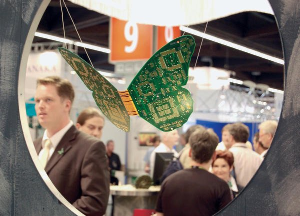
While the global electronics industrie suffers from the financial and economic crisis, Moore´s law still is driving electronics to further miniaturization – meanwhile beyond the IC level: 3D chip stacking with through silicon vias (TSVs) and other technologies on sub-system or module level gain in importance. Three international research institutes have teamed up to provide the tools and technologies for future generation electronics. The PCB sector will, as well, change dramatically.
Future microelectronic applications require significantly more complex devices, the Fraunhofer IZM (Berlin, Germany) states. Besides the on-going trend toward higher integration density and performance, there is also a demand for more functionality, e. g. by integration of mechanical, optical and biological functions. In line with this trend the ITRS roadmap predicts an increasing demand for systems-on-a-chip (SoC). SoC fabrication is based on embedding multiple technologies, but there are serious disadvantages: The chip partition with the highest complexity drives the process technology, leading to cost explosion of the overall system.
The IZM says, in the future the integration of highly complex systems has to be carried out more cost-efficiently, with a high degree of miniaturization and flexibility for the adaption to different application. A possible answer to this challenge are 3D system integrationtechnologies that enable the combination of different optimized technologies with the potential of low cost fabrication through high yield, smaller IC footprints and multi-functionality.
In addition 3D integration is an emerging solution to the wiring crisis caused by signal propagation delay both at board and at chip level, because it allows minimal interconnection lengths and the elimination of speed limiting intra- and inter-chip connects.
Fraunhofer IZM, the Korea Advanced Institute of Science and Technology (KAIST, Deajeon, Republic of Korea) and the Packaging Research Center (PRC) at Georgia Institute of Technology (Atlanta, USA) have teamed up to develop 3D integration and system technologies beyond the present research activities. The goal: Developing technologies that address the present needs in TSV, 3D stacking, interposer technology, and system needs of miniaturization and monolithic integration of components.
The research activities are important, because the success of 3D silicon integration depends on the availability of new methodologies and skills that are required to achieve acceptable design quality and productivity.3D integration is expected to be a serious alternative to below 45 nm technology to follow Moore at lower cost. Improvements of density of integration and performances will continue thanks to wire length reduction. Additionally, 3D enables an easier mix of technology in the same IC.
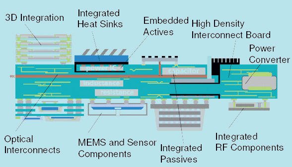
The substrate (PCB, LTCC) has to be as well subject to further development. The new 3D integration technologies have impact on the board as well. Smart substrate stacking allows the integration of devices based on very different packaging technologies like THT, SMT, COB, CSP, in a single stacked 3D package. A well established way of realizing substrate stacks is using TB-BGA (top bottom ball grid arrays) modules. The next generation of stacked substrates is coupled with the system in package strategy (SiP) and results in highly miniaturized hybrid microsystems. In afirst technological step the different PCB multilayers are assembled. Depending on the type of micro electronic components, SMT, chip on board (COB) or flipchip (FC) technology is used. In the second process, PCB sub-modules are connected by three dimensional soldering of PCB stacking frames (containing spacers and vertical leads), resuklting in a complete miniaturized microsystem.
Another way of deeper integration is the chip in polymer (CiP) technology. It offers a way to 3D system integration by embedding components into built-up layers of printed circuit boards. Thin chips of about 50 µm are die bonded to a substrate, e. g. FR4. By 3D stacking of layers with embedded chips an extremly high packaging density can be achieved.
All these technologies will change the standard workflow in electronics manufacturing dramatically. At best PCB manufacturers, chip- and package providers as well as the assembly industry cooperate densely and parallelise their processes. In about five years electronic industry looks different from now. The research process is going right now in this direction: It is more and more paralellised, what is not only prooved by the teaming up of the three mentioned institutes. While they are working hard on complex future challenges, most of their findings intruse in applied science research programs or even in available high tech products such like a miniaturized hearing aid and other medical devices with almost no delay.
Paralellised research and development activities
The Fraunhofer IZM department System Integration & Interconnection Technologies is currently working on a generic solution for nanophotonic packaging applications. Fiber pigtailing and packaging of nanowaveguide circuits are key technologies to realize nanophotonic applications. Technical problems start with a large mode mismatch of nanowires and standard single-mode fibers, which requires innovative coupling structures for low coupling loss and for large alignment tolerances. Looking further ahead, solutions are needed that allow for wafer level optical device testing and also for reduced packaging costs. These are essential ingredients for making nanophotonics a truly competitive and large scale technology.
3D-Sensor cubes with wireless intercom
As advanced microsystems, e.g., electronic sensor systems, are becoming more complex and individualized, standard state-of-the-art approaches will not be appropriate anymore to meet future objectives (cost, reliability, time to market, etc.). The innovative approach presented here will realize so-called electronic cubes, i.e., investigate and develop ultrasmall sensor cubes with dimensions of a few mm3 which are wirelessly communicating amongst each other. The objectives of the European project e-CUBES are to advance the microsystem technologies to allow for the cost-effective realization of highly miniaturized, truly autonomous systems for ambient intelligence.
The fabrication of e-Cubes with their need for high-level miniaturization can only be realized by system integration technologies, which use the third dimension: 3D System Integration. In order to achieve products with a large market potential, the main objective is to provide 3D integration technologies, which on the one hand increase the performance sufficiently and at the same time, allow for low-cost fabrication.
Smart High Integration Flex Technologies (SHIFT)
Development of smart, high-integration, mechanically flexible electronic systems, for a wide variety of applications is the objective of the VDE/VDI-IT SHIFT project. Smart means that the flexible multilayer laminate has embedded components, and that the different flex layers in the multilayer structure can have different functions, meaning that it might be necessary to combine layers of different base material in the laminate. Compactness of the resulting circuit will be boosted in two ways : by using the third dimension for electronic component integration (not only on front and back side, but potentially on every conductive layer) and by drastically increasing the wiring density through the introduction of new flex manufacturing and lamination techniques. Innovative technologies to be developed in SHIFT include
- a new, cheap flex laminate technology, based on a process for electroless Cu deposition on polyimide
- a new lamination technology, based on interconnection by solid state diffusion
- component embedding technologies : resistors, capacitors, RF components and ultrathin (20 micron) chips
- assembly technologies on embedded multilayer flex
The rationale of the project is that in order to realise the „ambient intelligence“ vision, more and more electronics systems will accompany the citizen. For these systems there is a trend towards increased functionality, compactness, wearability and reduced weight. The system may not hamper the mobility of the human carrier. Flexible electronics systems take the shape of the object onto or into which they are placed and may become quasi non-noticeable to the user. Compared to their rigid board counterparts they show a drastic increase of comfort for the user, and therefore the trend is starting and will become only stronger towards the use of „smart“ comfortable mechanically flexible electronic systems. The aim of SHIFT is precisely to develop enabling technologies for such complex flexible electronic systems.
Nuremberg shows future trends
The parallelizing and dynamic of R&D in electronics becomes highly apparent at the coming SMT/Packaging/Hybrid show and conference(may 3rd – 5th, Nuremberg): The international conference with tutorials which runs in parallel with the exhibition is the most important practice oriented platform for presenting new research results, applications and user reports within Europe’s microelectronics sector. Approximately 500 delegates will come to discuss the latest and future developments in the field of advanced assembly over the complete production chain from design and process technologies to innovative applications. The conference will be led by Herbert Reichl, professor at the Technical University of Berlin, their head of research in microperipherals and, as well, head of Fraunhofer IZM..
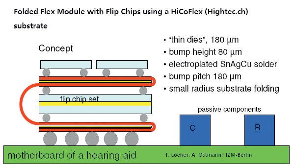
While the topic of this year’s conference is “Manufacturing of printed circuit boards based on flex and rigid-flex substrates“, the german VDE/VDI-IT shows on its group booth a actual working manufacturing line producing a communication board. On this board many mentioned integration technologies are realised. Another example is the miniaturized flex board of a hearing aid. By producing a standard 2D-flexboard and folding it to a 3D stack some advantages of 3D integration can even achieved with currently state-of-the-art technologies. In industrial sensors this first stage of 3D integratiopn is mainly used.
EPP EUROPE 406
Share:


