The global electronics industry has been aware of the pressure to create more environmentally friendly (green) products for a number of years. In the US, Japan and Europe, there are different strategies under way, driven by different legislative impetus, cost considerations or environmental awareness, respectively. It seems that Japan will probably lead in the early introduction of green mainstream board assembly operations, the US appears especially hesitant, and the European community has this step postponed remarkably.
Jeff Cannis, Senior Staff Engineer, Amkor Technology
While some may still wish to debate the logic and the costs acquainted with the introduction of manufacturing Pb-free or green electronics (or in some other ways more biological compliant products), there is no denying that a higher percentage of electrical devices, and the components that are used in their assembly, will have to be produced in green versions. The exact timing and extent of this conversion remains to be seen. However, a deep look into the global scenario reveals that millions of consumer products such as video recorders, home and telecom appliances, are already produced using environmentally compliant materials. Most subcontract assembly companies realize that to ignore this movement could potentially reduce market share, or at the very least damage relationships with customers.
Issues faced by the packaging industry
Obviously, the elimination or reduction of Pb is a key point. Component terminations, typically an SnPb-plated coating or SnPb-solder sphere, must be replaced with appropriate alternate materials. The elimination of internal Pb-containing materials for die-attach and flip-chip applications is less clear. Lead-free replacements have been identified for some of these internal packaging requirements. However, concerns regarding melting point hierarchy still need to be resolved or understood. There is also a possibility that exemptions or extensions may be granted for particular applications.
In addition to the removal of lead and the minimization of other toxic heavy metals such as copper, cadmium or mercury, brominated compounds used to suppress combustion must be eliminated, too. This directly affects mold compounds and PCB substrates used in packaging and board assembly. Coupled with the move to eliminate halogens is an implied requirement to stop using antimony (Sb) compounds. Although not specifically mentioned in legislation, most companies are including Sb removal in their programs.
As a final requirement, package reliability must be increased. The higher assembly temperatures used in Pb-free production processes will place increased stress on the package, making delamination and package failures more likely. The net effect of the move to environmentally friendly electronics is that most packages (and in turn many board assemblies) will undergo significant changes, if not a total redesign.
In order to meet the challenges of green packaging, the subcontract assembler must address a number of obstacles and uncertainties. Diversity of customers creates a range of product applications, variation in implementation timing and a variety of engineering solutions, and there are different legislative requirements by region. The lack of a standardized solution is further exacerbated by the fact that the industry is still assimilating data with respect to Pb-free soldering systems, and suffering from the absence of uniform specifications and product requirements. As companies are scrambling to provide products for the earliest deadlines, material and process decisions are being made before the database has been completely filled. The risk associated with this course of action will have to be properly managed, and evenly shared by the supply chain. It is likely that the effort to collect data will take years before the industry has a full understanding of all the key engineering and scientific issues. In the meantime, implementation will proceed.
From Amkor’s perspective, it is essential to provide appropriate packaging solutions to our customers in a standardized offering. By utilizing a combination of internal development programs, consortium activities and selected co-research efforts with key partners, it is our hope to present viable solutions to our customers, with the necessary supporting data. While expecting total agreement among all customers is unreasonable, limiting the material set options is desirable – not only from a logistical standpoint, but for quality and cost considerations as well. Multiple assembly-material options can add to the qualification workload, which can delay implementation. The use of more than one solder ball alloy will decrease the purchased quantity of any single alloy, thus increasing cost. The installation of plating lines in order to produce multiple lead-free coatings is also a costly proposition and adds to the logistical nightmare.
Solutions and packaging advances
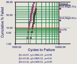
The Pb-free solders considered for use number in the hundreds. The down-selection process used by consortia and other industry participants varies from group to group and company to company. However, we are seeing some degree of commonality in the proposed solder alloy solutions. With only a few exceptions, the tin/silver/copper family of alloys appears to be gaining widespread acceptance. These materials typically melt in the range of 216 to 219°C, and have only minor variations in composition, as shown in table 1. Although there is still a search for a viable alloy that possesses a melting point close to that of eutectic SnPb solder (183°C), the thought of using a higher-temperature solution is becoming more palatable. This change in philosophy is a result of a number of factors. First, board level reliability of the Pb-free solder joint is at least as good as one made with eutectic solder, if not substantially better. Published thermal cycling data has typically shown a 20% or more improvement in thermal cycle performance. This is supported by evaluations performed by Amkor (see figure 1)
The second factor easing the choice of the SnAgCu alloys is that maximum reflow temperatures during board assembly may not reach the 260ºC level for many assemblies. A number of studies, including a few presented at the APEX 2001 conference, indicate that good solder joints can be formed with peak temperatures of no more than 245°C. This temperature is within the capability of many existing packages without having to make significant changes to the material set.
Another confusing factor in the selection of solder alloys has been the uncertainty of the patent situation. A number patent claims, primarily in the US and Japan, cover a wide range of SnAgCu alloys and their variations. The industry has been attempting to sort out the issues of „prior art“, priority date of the patents, and the exact coverage of each claim. As more and more data becomes available, it is clear that performance differences may not be significant within the family of alloys. Therefore, companies are attemptingto choose an alloy that will avoid any legal en-tanglements. The ideal situation would be forpatent holders and material suppliers to reachagreements allowing for worldwide distribution and use of the various SnAgCu alloys. That is in fact what is now happening in the supply chain. In any case, suppliers that eliminate this concern through appropriate licensing will occupy a commanding position.
For leaded packages, the situation is less clear. Since the typical method of application for the leadframe coating is electro-deposition, it is necessary to use a solution compatible with the existing infrastructure. Packaging solutions using pre-plated nickel-palladium (NiPd) technology have been in use for more than ten years. Although a proven technology, NiPd packaging does not appear to be gaining in popularity despite the increased pressure to eliminate Pb. It is still haunted by concerns over cost, consistent supply, board assembly issues and package reliability at higher reflow temperatures.
Instead, replacing the usual end-of-line solder plate process with a Pb-free version is favored, for a number of reasons. First, existing assembly process equipment and sequencing will remain unchanged. In addition, package reliability is expected to be equivalent to current levels since the same leadframe will be used and plating electrolytes are very similar to SnPb plating processes. This will also maintain cost parity with the existing SnPb assembly process.
So the only question is, which Sn-based deposit to use, or is pure Sn the answer? There is still a significant divergence in the industry in this area. A Japan industry segment is requesting SnBi, as it is believed that the inclusion of Bi will suppress Sn whisker growth. SnCu is also being considered by some for the same reason. Currently, there seems to be a groundswell of support growing for Sn. Companies with a long history of using Sn-plated packages are choosing to use matte Sn. As a long-term solution, Sn-plating appears to have the best chance of all the possible options. The main obstacle that remains is concerns over product-reliability issues due to Sn whiskers. Once a comprehensive understanding of the whisker mechanism is established, an accelerated aging method, along with techniques for the prevention or reduction of whiskers can be identified. Establishing industry-standard whisker criteria will go a long way toward stabilizing the situation with respect to Pb-free component finishes. Recent activity and research to investigate metallurgical structure and internal stresses may be moving the industry closer to this goal.
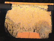
At the onset, one of the concerns expressed by many companies was with regard to package reliability, given that maximum component temperatures on a board assembly could reach 260°C. Visions of cracked and failed components permeated the industry (figure 2). I am happy to say that within the past two years those visions have begun to fade. Packaging materials that can meet a minimum of JEDEC Level 3 moisture sensitivity are obtainable for most package types. Not only are high temperature-capable materials available, but also many are also halogen-free.
These comments should not be meant to imply that all the technical issues have been conquered, but the industry has developed materials and processes that will allow green electronics implementation to proceed. This is quite an accomplishment considering the short timeline involved. It is also realized that board assembly processes may not be as severe as were initially anticipated. A well-controlled process, coupled with modern assembly equipment and proper board design, will permit lead-free soldering to occur at reasonable peak temperatures. The development work will continue for years to come, and the industry will fine-tune the packaging solutions as our understanding of these new systems grows.
Important cost issues
Although much of the effort for green electronics implementation has centered on technical issues, cost implications cannot be ignored. Unfortunately, there is no simple comprehensive formula for estimating the cost implications of going green. In certain packages, the improved performance required to meet Pb-free assembly can only be achieved by changing to materials that are more expensive. The use of pre-plated NiPd-leadframes can also bring additional material cost into the picture. Pb-free solder plating cost will be dependent upon the particular coating selected. Some of the proposed coatings, notably SnBi and SnAg, are more difficult to electroplate. These plating processes typically run at a slower rate than matte Sn, SnCu or the currently used SnPb process. For area-array packages, Pb-free solder sphere pricing can be as much as three to four times that of SnPb when purchased in low quantities.
The basic assembly processes remain very similar, and therefore are not expected to influence final cost significantly. Therefore, the main impact to packaging cost will originate from the materials. The exact impact will vary from package to package, as determined by the amount of change required to meet the higher requirements.
In summary, the movement towards green electronic products has provided a number of benefits:
• Improved package reliability
• Advancements in materials
• Companies take a much more critical look at the environmental impact of their activities
The major negative impact will be felt in the area of cost. Significant amounts of R&D expenses have been spent by the industry. Given the slow and prolonged implementation timing, it is expected that it will take many years to recoup those expenses. The extended conversion phase will also require assemblers to maintain dual manufacturing capability, both traditional and Pb-free products. Even if implementation stagnates or is reversed, there will be many residual benefits to the industry. Not the least is a renewed sense of cooperation within the entire supply chain.
How the main manufacturing regions dealing with ecological concerns
Progress in the European legislation has been slow, and has now created a complicated situation. Since the year 2000, after five years of draft documents and consultation on original WEE (Waste from Electrical and Electronic Equipment) proposal, the industry is facing three different items of EU legislation:
• WEEE – dealing primarily with minimizing waste and maximizing recycling at end-of-life
• ROHS – concerned with restrictions or bans on the use of hazardous materials (for example lead, cadmium or mercury, etc.). It requires such substances to be phased out of new products by 2006. Although there are some exemptions to this ban (lead in ceramic, glass, automotive electronics or for radiation protection), Pb-free processes are mandatory.
• EEE – dealing with minimizing overall environmental impact by adopting green design and manufacture, without ban of substances
There are no such impending material bans in other parts of the world, the emphasis being on recovery. Especially in Japan, impending legislation is not longer a driver. There is a buzz phrase in use (corporate environmental awareness). Maybe this is a euphemism for winning market share. However, this initiative is top-down driven, and corporations do build environmental performance (and in turn can expect rewards) in their plans. The JEITA roadmap indicates that full use of lead-free solder in all new products will be attained in the year 2003. Nevertheless, in China, the glitzy star on the Asian manufacturing sky, ecological concerns of this kind are still far away from entering the mind of people as a mainstream.
In the United States, the threat of legislation has been looming on the horizon since the early 1990s, and is documented in the Reid bill. (Senator Harry M. Reid, Senate Bill S391, 1991, Lead Exposure Reduction Act.) However, previously disinterested into lead-free soldering, the discussion in the US revolving around green electronic manufacturing is gaining even more momentum. Although much of its debate still centers around the apparent lack of any technological and financial sense in moving to Pb-free solder, there can be seen a growing common understanding in the industry to reduce the application of hazardous substances and processes in general. As a result, plenty of the basic research on green technology in electronics manufacturing is being carried out there.
ZUSAMMENFASSUNG
Die Industrie spürt den Druck, umweltverträglichere Produkte herzustellen. In den USA, Japan und Europa werden differierende Strategien verfolgt, hinter denen unterschiedliche Gesetzesvorlagen, Umwelt- oder Kostenbetrachtungen stehen. Japanische Hersteller werden ab 2003 alle Baugruppen „grün“ in hohen Volumen herstellen, in den USA wartet man noch etwas ab und Europa hat die offizielle Einführung bis 2006 verschoben.
RÉSUMÉ
L’industrie ressent la pression qui la pousse à fabriquer des produits plus respectueux de l’environnement. Les différentes stratégies suivies aux USA, au Japon et en Europe répondent à différentes législations et considérations liées aux coûts et à l’environnement. Les fabricants japonais produiront à partir de 2003 tous leurs modules électroniques „en vert”. Aux USA, on attend encore que quelque chose se passe et l’Europe a repoussé l’introduction officielle à 2006.
SOMMARIO
L’industria percepisce la pressione nella realizzazione di prodotti compatibili per l’ambiente. Negli USA, Giappone ed Europa si perseguono strategie differenti, dietro le quali si nascondono diverse prescrizioni di legge e considerevoli aspetti ambientali e di costi. I produttori giapponesi a partire dal 2003 produrranno tutti i gruppi costruttivi in formato „verde“ in ampi volumi, negli USA si preferisce aspettare ancora un po’, mentre l’Europa ha rimandato l’introduzione fino al 2006.
Share:


