Microfocus X-ray inspection has become a generally accepted method to control the quality of board assemblies, and to analyze defects of hidden solder joints. And it is key to efficient implementation and monitoring of the reflow process for BGA, CSP and flip-chip. For optimum exploitation, the right equipment should be operated in an appropriate way, and results be interpreted in light of the assembly process.
Dr. Holger Roth, Phoenix X-ray
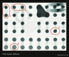
An X-ray image is generated by different X-radiation absorption of various parts of the object. Simply spoken, these absorption differences are due to variations in density or thickness of the object. For solder joints, mainly the thickness (or shape) is of interest. The longer the path of the radiation through a part of the object, the darker this part appears in the image. So, any defect that has a remarkable influence on a solder joint’s shape can be detected with X-ray technology. Some defects such as bridges can be „seen“ directly, others can be detected by their signatures that can be used to define test criteria as listed for a top-down view in the table.
The correspondence of the signatures to the various defects is known from experience, but can also be understood from simple geometrical considerations. For example, if a single BGA solder joint appears brighter than its neighbours, it is obviously not as thick and, hence, must be open (not properly soldered). If the joints in the center of a BGA are broader and brighter than those at the edges, most likely the package is more or less bowed (substrate or board warpage), and presses down the central joints so that they become broader and thinner. Figure 1 shows some examples of defects and their appearance in X-ray inspection.
Wetting analysis
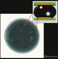
A more subtle task is the analysis of the wetting quality at both board and component pad which means to check whether the solder is really in contact with the pads. Again, a proper interpretation of the image can help. The related test criterion depends on whether the joining pad area is defined by a solder mask overlapping the pad or by the etched copper pad itself. In the latter case, well-wetted pads are embedded into the solder. In the X-ray image, characteristic dark rings at the edges of the pads are visible which are due to the additional solder in this area (figure 2). In the first case, the joining pads appear as dark circular areas if they are well wetted.
In practice, the related differences in thickness must exceed 2% of the absolute solder thickness to be visible with an image intensifier. Though this limit can be lowered to about 0.5% by using digital X-ray detectors, the signatures of wetting defects can be very faint in some cases and might be concealed by the barrel-shaped solder joint itself. However, the detectabilty for such fine structures can be enhanced remarkably by just reducing the absolute solder thickness to be penetrated, for example, to take an oblique view of the solder joints. In this way, not only the wetting status of the pads becomes plainly visible: the shape of the solder joint is clearly displayed, too.
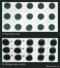
Figure 3a (top) shows fifteen solder joints of a PBGA in top-down view. Some of the joints at the lower left appear slightly brighter and broader than the others. This is a signature of opens according to which are described in the table. In figure 3b (bottom), the same solder joints are displayed in an oblique view. Here the opens can be clearly identified: the solder balls of the indicated joints are evidently not connected to the pads, and a sharp gray value step can be seen close to the board pad whereas the other solder joints fade out towards the board. The solder joint in the center (at the bottom) is not open but has only partially wetted the pad surface.
This strong verification method can also be applied to the smallest solder joints as present in CSPs or flip-chips by means of the OVHM-technique (oblique views at highest magnification) which avoids the loss of magnification typical for the customary tilt technique. For the smallest solder joints (flip chip) with diameters below 100 micron, the first nanofocus X-ray tube with a resolution of down to 0.5 micron is now available. With sufficient tube voltage (100kV or more) and appropriate focal spot size (less than 10 microns), microfocus or nanofocus X-ray systems are can provide images with the resolution and tonal accuracy demanded by IPC standards.
Bubbles inside joints
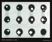
Voids are bubbles inside solder joints which appear as lighter spots in the X-ray image. The impact of voids on the reliability of solder interconnections has not been investigated in detail yet, but some studies are currently performed. Some earlier studies even point out that the reliability increases for solder joints that contain voids up to a certain size. Nevertheless, the standards IPC-A-610C (acceptability of electronic assemblies) and IPC-7095 (design and assembly process implementation for BGAs) define maximum void sizes for BGA solder joints. According to 610C, the maximum acceptable percentage of the ball-to-board interface area covered by voids should not exceed 10%, joints with more than 25% voiding are classified defect. IPC-7095 states values in the range of 9% to 36% depending on the vertical position of the voids and on the application of the assembly. In any case, the number of solder joints affected by voiding and the size of voids can indicate process control or improvements, and so it makes sense to measure bothby a suitable image processing software (figure 4).
Assemblies populated with BGAs providing nearly zero void percentage do exist, but there is no straightforward way to achieve this, since the void size in solder joints depends on a complex of process parameters including the formulation of the paste and the reflow profile. The mechanism of void formation, which would be key in suppressing, has not be definitely described yet and should be subject of further investigations.
Failure analysis can rely on the image quality of the X-ray systems (leading equipment will deliver superior images) and on a set of proven test criteria. However, process control requires the inspection of larger lots and a statistical evaluation based on automated procedures. The first step of automation is the preset evaluation of solder joint integrity by image processing software to achieve reproducible and quantified results. This now is no longer restricted to very big lots due to the immense programming time. An auto-setup software is available which can be also applied to small lots of merely 5 or20 assemblies, needing a short setup time of only a few minutes. Such software covers all the test criteria (see table), and can also be included in existing X-ray equipment. All results are listed in a file for eachball individually, using, for example, the JEDEC designations.
Stages of automation and SPC
The latest BGA software uses both top-down and oblique views as shown in figure 3 to detect and classify wetting defects automatically by means of a unique auto-calibrating algorithm. In a second stage of automation, this software can be combined with an auto-positioning system and, in a third stage, with a board handler to perform the inspection without interaction of an operator.
The X-ray inspection of BGA solder joints is mentioned in the described IPC standards A-610C and 7095 which already include many of the test criteria and their relation to the solder joint defects (listed in the table). The BGA acceptance requirements presently seem not to be as strictly quantified as for other solder joints – presumably because of lack of reliability data. Unfortunately, the standards refer to X-ray images whose quality is not really up-to-date so that the capabilities of this technology, namely of recently developed techniques such as OVHM and wetting analysis, are not exploited at all.
3D or 2D – is this the question?
X-ray 3D inspection of electronic assemblies customarily utilizes the principle of laminography in different digital and analog imaging processes. Laminography seemed very promising back in the beginning, but turned out to be ineffective in off-line and semi-automated inspection of concealed solder joints where a high image resolution is required: the time spending is in the range of 10 minutes (for about 20 solder joints), and in comparison to a 2D oblique view the detection efficiency for open joints is lower. Furthermore, unavoidable image artifacts complicate the interpretation. Nevertheless, automated 3D inspection techniques have been successful for double-sided assemblies. Here, 3D enables the detection at least of rough defects such as solder bridges, missing solder joints and deviations in diameter, even in areas that are hidden in top-down view.
In particular with the inspection of BGA and CSP solder joints up to now, no advantage in defect detection could be found which would justify the increased time consumption, especially since the most effective OVHM-technique can yield superior results within seconds. In off-line applications, laminography is useful wherever defect detection is impossible, even in oblique 2D views as, for example, in objects that consist of flat layers. In addition, laminography can be suitable to determine vertical positions and distances in broad flat objects. On account of its considerable time consumption, laminography for the time being will be restricted to laboratory applications.
Limits by contrast and patial resolution
For the detection of soldering defects such as bridging, faulty paste print, insufficient reflow, excessive voiding and mis-registration, microfocus X-ray 2D inspection is well-established. Starting out from a minimum prior knowledge about the configuration of pad and solder mask, the operator can determine the wetting status of the pads, provided that image quality of the X-ray system is sufficient in top-down as well as in oblique views. By means of evaluation algorithms, wetting defects can be revealed automatically with high efficiency. Though giving a good guideline, the recently published standards on BGA X-ray inspection neither definitely lay down acceptance criteria yet, nor do they exploit in full the capabilities of modern systems such as for wetting analysis.
Zusammenfassung
Wegen hoher Investitionskosten, der Länge der Prüfdurchgänge sowie dem nötige User-Training dürfte Röntgeninspektion in der Baugruppenfertigung nicht zum Mainstream werden. Aber wo es um Informationen über verborgene Lötstellen (geflippte Field-Array-Packages) und andere spezielle Baugruppenbereiche geht, ist X-Ray die erste Wahl in der Qualitätssicherung. Unterschiedliche Techniken erleichtern die optimale Applikation. Die im Prozeßmonitoring gewonnenen Daten finden zudem auch Verwendung bei der kontinuierlichen Verbesserung der Assembly-Prozeduren.
Résumé
En raison de l’importance des investissements, de la durée des contrôles et de la nécessaire formation des utilisateurs, l’inspection par rayons X ne va probablement pas s’imposer partout dans la fabrication de modules. Mais cette technique représente la meilleure solution en matière d’assurance qualité dès lors qu’il s’agit d’obtenir des informations sur les points de brasage inapparents (Field-Array-Packages) et d’autres endroits spécifiques des modules. Différentes techniques en facilitent et en optimisent l’application. Les données obtenues durant le contrôle du processus sont en outre utiles pour l’amélioration continue des procédures d’assemblage.
Sommario
A causa degli alti costi di investimento, della lungaggine delle procedure di controllo cosìccome dell’addestramento necessario per gli utilizzatori, nell’ambito della produzione di gruppi costruttivi il controllo a raggi X non si rivelerà un Mainstream. Dove però si tratta di avere informazioni su punti di saldatura a dolce nascosti (Field-Array-Packages di tipo flippato) e su altri gruppi costruttivi, il controllo a raggi X è lo strumento di prima scelta per l’assicurazione della qualità. Delle differenti tecniche agevolano un’applicazione ottimale. I dati evinti nel monitoraggio del processo trovano inoltre applicazione anche nel continuo miglioramento della procedure di assemblaggio.
Share:


