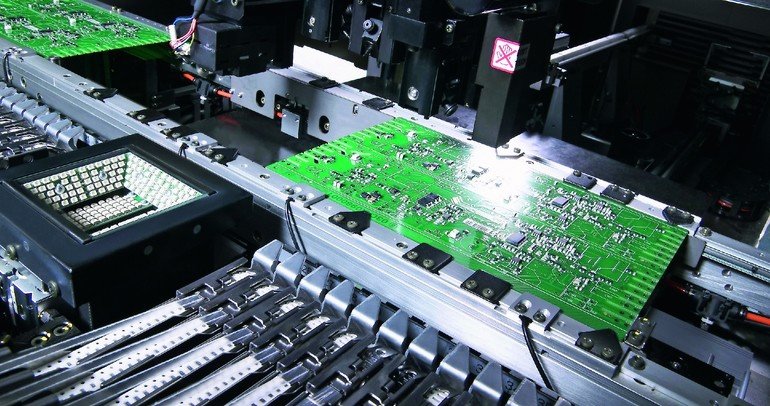


Boundary-scan, (aka IEEE Standard 1149.1) and its related specifications, has become the de facto standard for testing complex digital and mixed-signal designs during PCBA (printed circuit board assembly) manufacturing. While conventional test methods such as ICT (In-Circuit Test ) encounter difficulties due to lack of access (for probing circuit nodes) boundary-scan succeeds as it is essentially an embedded test resource that is designed-in from the start of the project.
JTAG Technologies, Peter van den Eijnden, Managing Director
What’s more as the quality of BSDL (boundary-scan model) files from the IC vendors, the level of automation of software and speed/quality of the controller hardware from the test tools providers have improved then so too has boundary-scan acceptance and adoption. Not so well known, however, are the consequential uses and working environments for boundary-scan, which if considered ‘holistically’, offers benefits throughout a given product’s life cycle and not just within manufacturing testing.
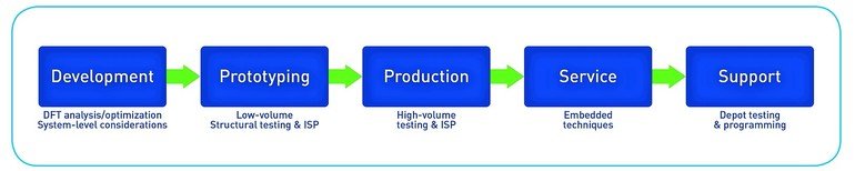
The product life cycle
As an electronic product moves through its life cycle, from development through prototyping to manufacturing and finally to the service and support phase, responsibility for the product also migrates through the organization. At the points of transfer from one department or discipline to the next, significant delays and disruptions can occur, brought on by a variety of issues.
One of the several issues that arise during the life cycle is the use of different test methods and tools among the various organizations. Failures of correlation can occur and put stress on inter-department communications. If problems are not rapidly understood and resolved, such vital aspects as time-to-market, repair turnaround time, and product quality and reliability quickly escalate beyond acceptable limits. Symptoms of problematic transfers are:
- Extra design cycles, caused by poor testability and/or manufacturability, often involving multiple layout spins and prototyping runs
- Long prototype debug intervals, caused in part by the presence of manufacturing faults obscuring design issues
- Logistical difficulties with pre-programmed devices, such as wrong or out-of-date configurations being placed on PCBs
- and causing assembly delays
- Problems in manufacturing fault clearing caused by poor test diagnostics and/or wrong documentation
- Oversized bone-pile at functional test and excessive time expended in PCB troubleshooting, due to prevalence of defective boards making it through structural testing,.
- Mystery failures in HASS or HALT environmental tests, e.g. failures at temperature that disappear at room temperature
- Lengthy repair times due to poor test capability in the support facilities
- Boundary-scan can help resolve many of the issues discussed above. Furthermore, significant economic opportunities and quality improvements accompany these benefits. The technology is particularly effective if it is implemented corporately as a fundamental part of the test strategy.
The life cycle aspect
Use boundary-scan tools to achieve Design-for-Testability goals
Using boundary-scan coverage analysis tools early in the product cycle pays off in reduced time to market and improved product quality. The designer will know, prior to prototyping, the level of test coverage that will be attained with the product. If the coverage is deemed to be inadequate, the design can be modified and coverage re-examined, avoiding the delays that every subsequent process step would otherwise encounter. By adopting a policy in which the design phase must include DFT analysis that meets coverage requirements, the organization will avoid wasted layout spins and prototype builds.
Test prototypes more efficiently
Unlike structural test methods such as in-circuit testing, boundary-scan testing requires minimal fixturing. Therefore, boundary-scan can easily be applied to small prototype runs allowing detection and rapid repair of structural faults. Screening for structural faults enables the designer to properly focus on design issues during the critical prototype stage. Boundary-scan can even provide access to a large set of test points for electrical stimulus and sensing during debug, as well as a convenient means of rapidly programming (and re-programming) flash and logic elements on the board during firmware verification. The ease with which boundary-scan applications can be developed means that design revisions can be quickly incorporated in the test and programming routines.
Optimize structural testing
Boundary-scan improves production test efficiency in several important ways. Scan-based tests typically run at high speed (on the order of tens of seconds even for highly complex PCBs) and are capable of producing pin-point diagnostics. Fixturing for test access can be dramatically simplified, if not eliminated entirely. Furthermore, the modular nature of boundary-scan allows it to be combined with many other structural test methods, such as in-circuit testing or flying probe, which may already be in use in the factory.
Pre-screen boards prior to functional test
Boards with faults that are not detected by structural testing are said to “escape” to the functional test stage. Escapes are readily detected in functional testing, but not so easily corrected. An unfortunate, highly undesirable result of functional test failures that cannot be diagnosed and repaired is the bone-pile. Boundary-scan helps minimize the bone-pile by assuring that no (or very few) manufacturing defects escape to functional testing. Using boundary-scan as a precursor to functional test pays off by reducing the amount of time that designers must devote to troubleshooting difficult to diagnose boards. Because of the precise diagnostics from boundary-scan, board repair requires only one action rather than several (trial and error in the case of functional test repairs). This precision will have a significant positive impact on product reliability, and reduction of product-to-market times.
Program flash, PLDs, and other devices after PCB assembly
The same tools used for boundary-scan testing can also perform high-throughput in-system programming (ISP) of flash memories , a wide variety of programmable logic devices and devices with embedded memory (e.g. microcontrollers). Programming is performed after board assembly at the optimal point in the flow, and reprogramming can be performed easily without having to remove devices from the board. Savings result from reducing the number of tools in use, avoidance of IC sockets, and simplifying the process flow.
Enhance the effectiveness of environmental stress testing
Use of boundary-scan can significantly improve the effectiveness of HASS or HALT stress testing. Because the boundary-scan interface to the target is implemented over a thin cable which is highly impervious to interference, the test set-up is straightforward. Furthermore, boundary scan testing can be set to run continuously so that environmentally-induced failures will be detected and the fault data collected on the spot and time-stamped for later diagnosis. Intermittent faults which might occur only at elevated temperatures, for example, are captured, avoiding no trouble-found situations and preventing escapes to the functional test step, or worse, to the field.
Combine boundary-scan and functional testing
Integrating these complementary methods within one platform can provide major benefits to the manufacturing enterprise. Savings result from reduced product handling; fewer test stations, less floor space, a reduction in training requirements, and use of a familiar, unified GUI to the operator.
This technique is examined in more detail in a later section.
Implement boundary-scan at system level
Boundary-scan technology can also be considered for system level application for both test and in-system programming. This can be performed using either an external tester or embedded boundary-scan architecture. In both cases, control of the system level applications can be conducted remotely.Commercial ICs and software are available that enable such boundary-scan control to be designed into the target system itself, which is then capable of executing applications without the need for external control. This advanced architecture can be employed to advantage in maintaining test and programming access to in-service systems.
Use boundary-scan in repair
Centralized as well as distributed repair facilities can use the same boundary-scan-based tests as the factory, helping avoid correlation problems in analyzing test results. Furthermore, because boundary-scan requires almost no custom test set-ups, the repair department can rapidly switch between target types and versions in high-mix situations. In summary, if the product has been well planned, including observing the principles of design-for-testability, the enterprise will experience many, if not all, of the above benefits. Transitions of responsibility from one organization to the next are streamlined, inter-departmental communications are enhanced, and correlation problems are avoided by the use of a common test methodology.
Boundary-scan based functional testing
One specific aspect of enhancing the product life-cycle with boundary-scan is its integration within functional test. Both test methods fulfill the necessary quality assurance steps for the anticipated fault spectrum:
- Boundary-scan for manufacturing faults, typically caused by soldering problems
- Functional testing for at-speed problems, faults that are manifested at operating range limits, user-generated errors, etc., in other words the types of faults anticipated in actual use
Though distinct and complementary in purpose and methodology, the two techniques, boundary-scan and functional testing, can be combined with great effectiveness using a number of test system platforms, such as: PCI, USB, Ethernet, LXI or PXI(e) architectures. In recent times a ‘half-way house’ has also been developed known as JTAG Functional Test (JFT) whereby JTAG/boundary-scan access to digital and mixed signal circuit elements is scripted in a Python code program. Use of JFT enables a ‘boundary-scan only’ solution to test parts such ADCs DACs or complex logic clusters that rely on conditional branching decisions. Scripts can also be further enhanced by adding (processor) core emulation test capabilities with CoreCommander functions.
In this scenario, boundary-scan vectors for testing, JFT scripts and ISP of PLDs and flash, developed for use in the prior prototyping phase, are ported to the production environment and are driven to the board by means of the chosen boundary-scan instrument in the functional test chassis.
The boundary-scan operations can easily be integrated into the functional test environments such as custom GUIs or industry standards (TestStand, LabVIEW, and others). The controller drives the vectors to the target and collects the results. If failures have been detected, they are analyzed with the same diagnostic routines available to the designer. JTAG/boundary-scan ISP applications can then be executed to ‘breath life’ into the target prior to the next test phase.
After the boundary-scan applications are run, and assuming they run satisfactorily, the test management software proceeds to the next steps in the pre-programmed sequence, for example a set of functional tests such as temperature profiling, parametric measurement, electromechanical verification, etc. On the other hand, if the boundary-scan tests fail, then scan diagnostics, and possibly visualization tools, direct the repair to the point(s) of failure. If in-system programming only is also required, these steps can be performed after the structural test.
The advantages of combining the two methods within a test system are:
- Reduction in process steps and simplified product flow
- One-stop for structural and functional testing, and in-system programming
- Saving of factory floor space
- Reduced training requirements for test personnel with a uniform user interface
Boundary-scan offers a compact footprint, high performance, and broad availability of instrument types, including PXI(e)-based boundary-scan instrumentation. Typical Scan instruments allow up to four individual targets to be tested and programmed, and for extremely high volume production requirements, multiple boundary-scan controllers can be deployed, all running from a common test/programming source.
Testing is too often considered a test adder with no value-add proposition. However, this viewpoint ignores the real and substantial savings that can be realized with a well-conceived test strategy. The test strategist should consider the life-cycle issues described above in which measurable cost savings can be achieved by use of boundary-scan, and which can be enhanced by combination with functional test.
Combined testingdeliverseconomic benefits
Share:


