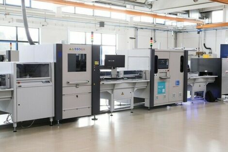
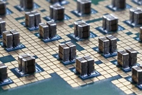
DEK has developed a high-throughput backside wafer-coating process, hosted on a stencil-printer platform, and capable of exceeding the ±12.5µm total thickness variation (TTV) stipulated by wafer specialists. The procedure is compatible with underfill or adhesive-type coatings, normally applied at a nominal 50µm thickness to the backside of wafers ahead of singulation. TTV is seen as the critical factor for backside-wafer coating. DEK’s ability to meet the established criteria opened opportunities for semiconductor packaging specialists to increase throughput and reduce the cost-per-package by using high-accuracy printing. The process is compatible with metal stencil and emulsion-screen technologies. Metal stencils enable materials with larger filler particles, such as encapsulation substance, to be applied with a smooth surface finish. Mesh stencils allow other materials such as thermoplastic adhesives to be deposited accurately and at high speed. In each case, the capability is there to achieve control over print thickness and ensuring uniformity. The turnkey process is ready for customers to use immediately; the company’s process engineers are reportedly able to deliver a full implementation service at customer sites worldwide. They are intimately familiar with the impact of stencil technology, thread size, emulsion thickness, metal thickness, squeegee or ProFlow selection, and machine parameter settings, when implementing this backside-wafer process.
EPP EUROPE 434
Share: