Homepage » Allgemein »

Acoustic imaging of bonded wafers

Allgemein
Acoustic imaging of bonded wafers

Acoustic imaging of bonded wafers
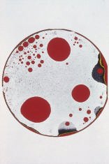
Sonoscan’s AW2000 systemfor automated inspection of bonded wafer can handle objects up to 200mm in diameter, which is especially useful in imaging after initial Van-der-Waals bonding. After this process, the wafers are joined only by weak chemical forces, and can be easily separated. Separated wafers are cleaned and then rebonded. Inspection at this point avoids further processing of defective wafer pairs. Automated acoustic imaging also serves as a process monitor for the initial bonding step. The system classifies inspected wafers, and is capable of imaging defects having sizes as small as 5 to 10µm. If needed, acoustic imaging can also be performed after annealing and thinning.

Current Issue
Titelbild EPP EUROPE Electronics Production and Test 11
Issue
11.2023
READ
Newsletter

Subscribe to our newsletter now

Webinars & Webcasts

First hand technical knowledge

Whitepapers

Find all current Whitepapers here

Videos

Find all current videos here


Industrie.de Infoservice
Vielen Dank für Ihre Bestellung!
Sie erhalten in Kürze eine Bestätigung per E-Mail.
Von Ihnen ausgesucht:
Weitere Informationen gewünscht?
Einfach neue Dokumente auswählen
und zuletzt Adresse eingeben.
Wie funktioniert der Industrie.de Infoservice?
Zur Hilfeseite »
Ihre Adresse:


Die Konradin Verlag Robert Kohlhammer GmbH erhebt, verarbeitet und nutzt die Daten, die der Nutzer bei der Registrierung zum Industrie.de Infoservice freiwillig zur Verfügung stellt, zum Zwecke der Erfüllung dieses Nutzungsverhältnisses. Der Nutzer erhält damit Zugang zu den Dokumenten des Industrie.de Infoservice.
AGB
datenschutz-online@konradin.de