The trend for miniaturisation of high-tech products is entrenched and beyond question. Of course, everyone wants smaller stuff, and for a multitude of reasons: portability, wearability, and style are key concerns among consumers, while on the other hand space is increasingly precious in server rooms and data centres that must deliver increasingly compute-intensive services, to growing numbers of users, in less than the blink of an eye. Meanwhile, the IoT continues to roll out, perpetuating an expectation to be able to interact with smart “things” everywhere, throughout factories, cities, and infrastructures. And then there is the automotive world, unrelentingly demanding more and more intelligent features and on-board systems; all within utterly unrealistic constraints on size, weight, and power.
The fact that our industry has been able to satisfy these demands, so far, is beyond remarkable. Much is attributable to progress in line with Moore’s Law, putting vastly more computing power onto ever-shrinking dies, with the related effects on power-supply sizes, signal speeds, and interface bandwidth. In today’s post-Moore era, maintaining the trend demands innovation in every aspect of the system, from 3D chip design to save silicon floorspace to PCB fabrication and component packaging.
Packaging
Packaging serves today’s manufacturing models. It’s the medium that enables the various component parts – including processors, power semiconductors, passives, etc – to be made in different factories by companies with different specialisms and configured and integrated by organisations that have their own competencies, like system design and, ultimately, production.
In the post-Moore era, component packaging is as urgent a target for miniaturisation as any other aspect of the system. Minimising packaging overheads not only helps build smaller systems but also contributes to performance improvement by reducing associated parasitic effects, like electrical resistance that causes power loss and self-heating, and thermal resistance that impairs dissipation.
In an ideal world, we want packaging to go away, and there is precedent for this. It’s what FPGA manufacturers have been doing for years by making it possible for designers to absorb the functions otherwise implemented in multiple discrete ICs into one single – albeit relatively large – device. Direct-bond assembly employed in power modules is another example, increasingly prevalent with the rapid adoption of electric drive into today’s vehicles. In addition, the case is frequently made for embedding passive components such as decoupling capacitors directly in PCBs. This can, potentially, save space and enhance reliability, although the possibility has been discussed for some time without becoming reality. It remains an innovation we await eagerly and may see in the near future as innovations in materials science and fabrication processes take us closer to a solution.
Having wished packaging into non-existence, in the real world it is, of course, incredibly important and is a key area for research to drive ongoing miniaturisation; especially now that advancing chip lithography, alone, is not able to deliver the progress we need. Its growing importance is underlined by the fact that foundries and integrated device manufacturers (IDMs) are beginning to drive innovations in this area. Historically, it has been the unchallenged territory of outsourced semiconductor assembly and testing (OSATs) or semiconductor packaging, assembly, and testing (SPATs) companies.
Challenge
The race is on to miniaturise packaging and it will likely be delivered through various means. These include 3D packaging that relies on techniques such as hybrid bonding, as well as technologies that simplify construction such as fan out wafer-level and panel-level packaging (FOWLP and FOPLP), which require no substrate or solder contacts. The importance of packaging presents opportunities for innovators to take the lead and create the new package layouts, construction techniques, and materials that will enable miniaturisation to maintain its fast pace in the future.
On the other hand, package miniaturisation presents tough challenges for manufacturing processes like printing and placement. These processes must deal with the effects of finer features, smaller solder deposits, reduced tolerances on placement accuracy, greater sensitivity to the soldering process settings and issues like paste particle size. Automatic optical inspection, also, is under pressure, to inspect finer features and handle increased component-placement density. These changes demand greater optical resolution, extra camera angles and better lighting, upgraded inspection algorithms, and faster performance to handle larger numbers of captured high-resolution images.
PCB fabrication is also under pressure as pad sizes, layer thickness, trace width, and trace gaps are also all being reduced. Drilling diameters for through-holes and vias also becoming smaller. Industry groups like the High-Density Packaging Users Group (HDPU) are studying the effects of extremely small PCB feature sizes on critical aspects of assembly performance, like reliability.
In Asia, still the dominant manufacturing destination for high-volume consumer products like smartphones, tablets, PCs, the smallest 0201 SMD chips, and chip-scale IC packages are routinely placed and inspected. This also demands fabrication of PCBs with extremely fine feature sizes. As a result, manufacturers based here are highly accomplished in terms of their investment in equipment and the process knowledge to achieve high yield rates at these smaller sizes.
Europe’s high-mix/low-volume manufacturing model invites more conservative designs that make setting up and managing production processes easier. Fewer manufacturing contracts require working with the smallest component sizes. The low volume demand makes it less viable to spend time and effort fine-tuning the processes to use those parts that have the smallest feature sizes.
However, we can say of life in general, in our globalised world, that what’s “over there” is soon “over here”. On that basis, Europe’s manufacturers can expect to have to deal with highly miniaturised packages and high-density PCB interconnects before long. They now need the courage to make the necessary investment in equipment and knowhow.
There is another trend that will demand greater ability to handle the cutting-edge miniaturised parts, and that is the opportunity for reshoring. There have long been calls to “bring manufacturing home” to Europe. In today’s world, post COVID, the arguments may be stronger than ever. The weaknesses of long supply chains have been painfully exposed and continue to be felt. The image of the Ever Given – grounded in the Suez Canal loaded with many millions of Dollars of offshore-manufactured products destined for western markets literally floating in limbo – made a persuasive argument for a more robust, localised model. Contemplating the effect of the blockage on other shipping at either end of the canal and in ports worldwide, also unable to move as a consequence, strengthens the case even further. Subsequently, the meteoric increase in shipping-container costs, economic effects of the Ukraine conflict like rising costs for fuel and raw materials, and ongoing environmental concerns, have added to the arguments that put reshoring firmly back on the agenda. Rising labour costs in offshore destinations add a further dimension to the argument.
EU governments are keen to welcome manufacturing back to their shores. This has been the case for some time: a report on reindustrialising Europe to promote competitiveness and sustainability, adopted by the European Parliament in 2014, supported reshoring initiatives and noted that one industrial job creates about two associated jobs in supply and service sectors.
Opportunity
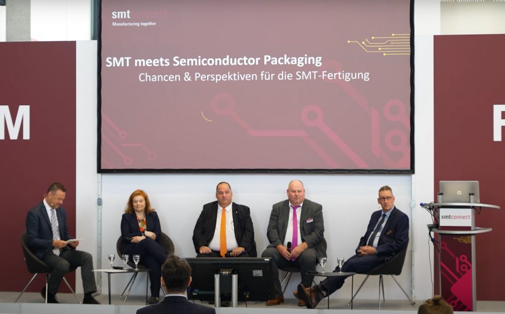
It’s a tremendous opportunity for European manufacturers, and one that has not escaped the attention of panel members at May’s SMTconnect 2022 roundtable discussion entitled: SMT meets Semiconductor Packaging – Opportunities and prospects for SMT manufacturing. Their companies are among those calling for brave investment as well as offering solutions and support for advanced assembly and inspection processes.
The roundtable group, comprising Torsten Vegelahn of EKRA (part of Asys), Michael Zahn of Christian Koenen, Harald Eppinger of Koh Young, and Dr. Tanja Braun of Fraunhofer IZM, were also mindful of the challenges that must be overcome. One is that the supporting ecosystem necessary for a vibrant high-tech manufacturing activity has become severely weakened, in the absence of the high-volume, cutting-edge manufacturing that has moved offshore. Getting that back is not an overnight task. And, of course, there is the demand for investment in improved capabilities and process knowhow to get the processes up and running in high volume and at high speed.
In addition, manufacturers planning to restart operations in Europe must also expect to maintain high standards of environmental protection, and for their performance in this regard to be scrutinised. On the other hand, there is investment on offer, through initiatives such as the European Chips Act that aims to increase the EU’s share of global semiconductor production. There is already world-class design knowhow, test expertise, and advanced research here. Now, the EU wants to invest upwards of €43 billion to ensure that Europe produces 20% of the world’s chips by 2030. This could provide an enabler for that much-needed ecosystem, and a catalyst for advanced package design as a defining capability of a world chip manufacturing power.