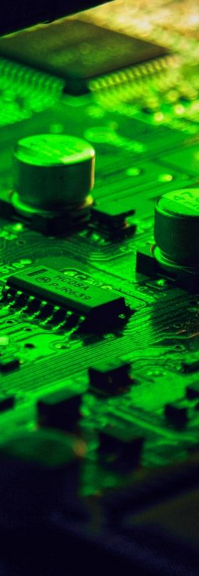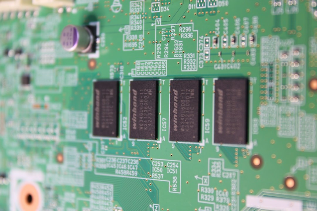
Modern printed circuit board assemblies increasingly rely on area-array packages such as BGAs, LGAs, QFNs and stacked PoP devices, where every single solder joint is hidden beneath the component body after reflow. Automated optical inspection, however capable, cannot see through a package. This fundamental geometric constraint makes X-ray-based inspection the only non-destructive method capable of verifying joint integrity, voiding levels and bridging in these configurations. At the same time, X-ray inspection is neither universally applicable nor infinitely capable: its value depends entirely on a clear understanding of what the underlying physics can and cannot reveal.
The following sections outline the physical principles of X-ray image formation, the distinction between 2D and computed-tomography (CT) approaches, the most common defect classes detectable by AXI, the practical limits of the technology, and the process-control logic that determines how X-ray fits into a complete inspection strategy.
How X-ray images are formed: attenuation and contrast
X-ray inspection exploits the differential attenuation of ionising radiation as it passes through materials of varying atomic number (Z) and density. Tin-silver-copper (SAC) solder alloys contain elements with relatively high Z values — tin (Z = 50) in particular attenuates X-rays strongly, producing high contrast against the FR4 laminate substrate (predominantly carbon, hydrogen, oxygen; low Z) and the copper conductors beneath. The result is a grey-scale image in which solder joints appear as distinct, bright regions that can be evaluated for shape, size, continuity and internal structure.
The X-ray source generates a cone-beam or fan-beam of photons; a flat-panel detector or image intensifier captures the transmitted intensity. Magnification is achieved geometrically: moving the board closer to the source and further from the detector increases the projected image size, allowing sub-micron effective pixel resolutions in high-end systems. Tube voltage — typically between 80 kV and 160 kV for board-level inspection — must be matched to the assembly: too low and thick copper planes absorb all radiation before it reaches the detector; too high and contrast between solder and substrate disappears.
2D radiography versus computed tomography: capabilities and trade-offs
Standard 2D X-ray (radiography) projects the entire assembly onto a single plane. This is fast and adequate for many defect classes, but it superimposes all layers of the board: a void in a BGA joint may be partially obscured by a copper pour on an adjacent layer, and bridging between closely pitched balls can be difficult to distinguish from overlapping projections. Oblique-angle imaging — tilting the source or the board — partially resolves depth ambiguity and is routinely used to separate ball rows in BGA packages.